Photoetching patterning method with micro-transfer patterned graph as mask plate

A photolithographic patterning and patterning technology, which is applied in the direction of photoplate making process, optics, and optomechanical equipment on the patterned surface, can solve the problems of low patterning accuracy and complicated processing process

Inactive Publication Date: 2007-01-03
CHANGZHOU INST OF ENERGY STORAGE MATERIALS &DEVICES
View PDF1 Cites 12 Cited by
  • Summary
  • Abstract
  • Description
  • Claims
  • Application Information

AI Technical Summary

Problems solved by technology

The multilayer structure generally has a complicated processing process, and different layers need to be patterned separately; while the negative pho

Method used


Image

  • Photoetching patterning method with micro-transfer patterned graph as mask plate
  • Photoetching patterning method with micro-transfer patterned graph as mask plate
  • Photoetching patterning method with micro-transfer patterned graph as mask plate

Examples


Embodiment 1

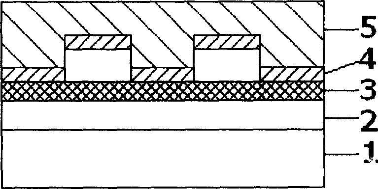
[0021] (1) Deposit a gold film 4 on the surface of the patterned polydimethylsiloxane soft stamp 5 .

[0022] (2) Coating a photoresist film 2 on the silicon wafer 1, after drying the photoresist film 2, coating a layer of polystyrene film 3 on the surface of the photoresist film 2 and drying.

[0023] (3) Fit the polydimethylsiloxane soft stamp 5 with the gold film 4 deposited on the surface to the surface of the polystyrene film 3, heat the whole system to 100° C., and keep it for 5 minutes. Then the temperature of the whole system was lowered to 20° C., and the polydimethylsiloxane soft stamp 5 was peeled off to obtain a polystyrene film 3 with a gold film pattern 6 on the surface.

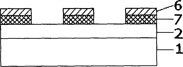
[0024] (4) The polystyrene film 3 with the gold film pattern 6 in step (3) is carried out oxygen-reactive ion etching, and the polystyrene film 3 without the gold film pattern 6 on the surface is etched and removed to obtain a polystyrene film Pattern 7.

[0025] (5) The silicon wafer 1 proce...

Embodiment 2

[0027] (1) Deposit a gold film 4 on the surface of the patterned polydimethylsiloxane soft stamp 5 .

[0028] (2) Coating a photoresist film 2 on the ITO glass 1, after drying the photoresist film 2, coating a layer of polystyrene film 3 on the surface of the photoresist film 2 and drying.

[0029] (3) Fit the polydimethylsiloxane soft stamp 5 with the gold film 4 deposited on the surface to the surface of the polystyrene film 3, heat the whole system to 110° C., and keep it for 3 minutes. Then the temperature of the whole system was lowered to 30° C., and the polydimethylsiloxane soft stamp 5 was peeled off to obtain a polystyrene film 3 with a gold film pattern 6 on the surface.

[0030] (4) The polystyrene film 3 with the gold film pattern 6 in step (3) is electrodeposited a layer of metal copper in copper sulfate solution, then the polystyrene film 3 with the gold film pattern 6 that has been electrodeposited copper Oxygen reactive ion etching is carried out, and the poly...

Embodiment 3

[0033] (1) Deposit a gold film 4 on the surface of the patterned polydimethylsiloxane soft stamp 5 .

[0034] (2) Coating a photoresist film 2 on the glass 1, after drying the photoresist film 2, coating a layer of polystyrene film 3 on the surface of the photoresist film 2 and drying.

[0035] (3) Fit the polydimethylsiloxane soft stamp 5 with the gold film 4 deposited on the surface to the surface of the polystyrene film 3, heat the whole system to 120° C., and keep it for 1 minute. Then the temperature of the whole system was lowered to 50° C., and the polydimethylsiloxane soft stamp 5 was peeled off to obtain a polystyrene film 3 with a gold film pattern 6 on the surface.

[0036] (4) The polystyrene film 3 with the gold film pattern 6 in step (3) is carried out oxygen-reactive ion etching, and the polystyrene film 3 without the gold film pattern 6 on the surface is etched and removed to obtain a polystyrene film Pattern 7.

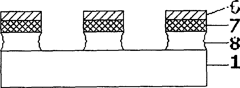
[0037] (5) The glass 1 treated in step (4) is...


PUM


Abstract

The invention is concerned with the photoetching design method that uses the micro-shift design as the covering-film board. The film structure consists of the metal film, the thermosplastic macromolecule film, the photoetching rubber film. The metal film design that is gotten by the method of the micro-shift design can be the following photoetching covering-film board, comparing with the traditional multi-layer structure photoetching design, omits once photoetching processing. The metal film design can ensure the peeling technics to get the transfer design with the matching size even the exposal time or the developing time appears windage, because the up-layer design metal film is not affect by the exposal and the developing process. The method can get the photoetching rubber sidewall structure that the edge is erect and sunken entad, therefore the photoetching design can use for the separator of the organic radiation layer and the pole layer that shows by the organic radiation matrix. The process precision is smaller than 1 micron that is higher than the design precision with the 10 micron negative photoetching rubber.

Description

technical field [0001] The invention belongs to a photolithographic patterning method, in particular to a photolithographic patterning method using a micro-transfer patterned pattern as a mask. Background technique [0002] In the electronic industry processing, photolithographic patterning technology is a mature micropattern processing method. With the development of organic electronics technology, photolithographic patterning technology is also applied to the field of organic electronics. In the photolithographic patterning process of electronic devices, in order to ensure the quality of the final pattern, it is necessary to obtain a photoresist microstructure with neat and upright edges and a small deviation from the pattern size of the photolithographic mask, so as to ensure the use of photolithographic pattern transfer. The precision of the resulting lift-off or etch pattern. In an organic light emitting matrix display, it is even required that the sidewall of the pho...

Claims


Application Information

Patent Timeline
IPC IPC(8): G03F7/00
Inventor 韩艳春邢汝博于新红
Owner CHANGZHOU INST OF ENERGY STORAGE MATERIALS &DEVICES
Why Eureka
Try Eureka