High-temperature resisting one-chip integrated micro-sensor structure and system integrating method

A monolithic integration, micro-sensor technology, applied in microstructure technology, microstructure devices, manufacturing microstructure devices, etc., can solve problems such as inapplicability, achieve low production cost, achieve miniaturization, improve space utilization and reliability. sexual effect

Inactive Publication Date: 2007-01-03
UNIV OF ELECTRONICS SCI & TECH OF CHINA
View PDF4 Cites 4 Cited by
  • Summary
  • Abstract
  • Description
  • Claims
  • Application Information

AI Technical Summary

Problems solved by technology

[0022] However, this patent is only applicable to monolithic MEMS when the microstructure is composed of polysilicon, and it is not applicable to other materials such as ferroelectric and piezoelectric microstructures.

Method used


Image

  • High-temperature resisting one-chip integrated micro-sensor structure and system integrating method
  • High-temperature resisting one-chip integrated micro-sensor structure and system integrating method

Examples


Embodiment Construction

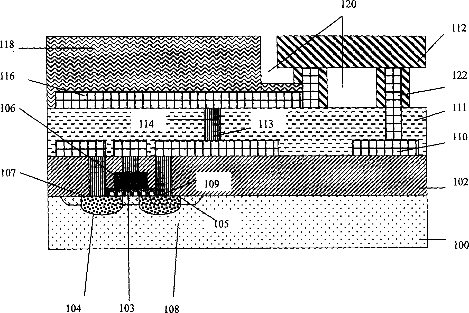
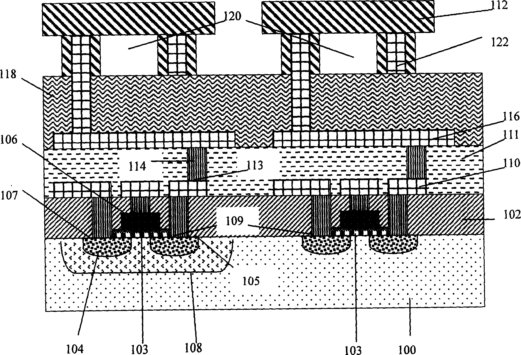
[0045] The invention proposes a monolithic integration method of "manufacturing IC first and then microstructure". This method is compatible with the standard CMOS process. The multilayer interconnection line of the integrated circuit is made of refractory metal silicide or refractory metal. After the IC is completed, the microstructure is made on the same plane, that is, the microstructure and the IC circuit are on the same plane, or in the same plane as the IC circuit. IC is the substrate, and microstructures are fabricated vertically to form monolithically integrated arrays or multifunctional microsensor systems.

[0046] see figure 1 .

[0047] First, SiO is oxidized on the cleaned silicon substrate 100 2 The film 102 is used as a field oxide layer, and the photolithography or etching process is used to open concave holes on the field oxide layer to define the specific positions of the source, drain and gate of the MOS transistor, and the N or P well 108 is formed by a d...


PUM


Abstract

High temperature resistant single scale integration microsensor structure and system integration method relates to integrated circuit technique in particular relating to single scale integration microsensor technology. It contains IC layer and microarchitecture layer, adopting refractory metal or refractory metal silicide as interconnection line. Said invention has advantages of overcoming microsensor system temp. limiting in single scale integration, raising integrated circuit space utilization ratio and reliability, realizing total system miniaturization and compatibility with existing production line.

Description

technical field [0001] The invention relates to integrated circuit technology, in particular to monolithic integrated micro sensor technology. Background technique [0002] Monolithic integration of microsensors on an integrated circuit (IC) basis can improve overall performance, reliability, and reduce size and cost. For example: monolithic integration can reduce the number of input and output pads in complex systems, enhance the drive and control of micro-actuators, improve the signal-to-noise ratio of the system, and help mass production. [0003] However, the monolithic integrated microsensor system faces the challenge of material and process compatibility. For example, in the MEMS manufacturing process, an annealing process higher than 1000 ° C is required to relieve the stress of polysilicon; Annealing at a temperature of 600°C can obtain ferroelectric properties. However, the traditional IC uses aluminum as the metal interconnection, but it can no longer work normal...

Claims


Application Information

Patent Timeline
Patent Type & Authority Applications(China)
IPC IPC(8): H01L27/04H01L23/532H01L21/822H01L21/768B81B7/02B81C1/00
CPCH01L2924/0002
Inventor 李平阮爱武胡滨
Owner UNIV OF ELECTRONICS SCI & TECH OF CHINA
Why Eureka
Try Eureka