
Semiconductor device

A semiconductor and high-voltage technology, applied in static memory, instrument, information storage, etc., can solve the problems of rising, shortening the life of storage unit, and insufficient precision of screening test, etc., and achieve the effect of stress relief and precision improvement

Inactive Publication Date: 2007-01-10
ROHM CO LTD
View PDF2 Cites 0 Cited by
  • Summary
  • Abstract
  • Description
  • Claims
  • Application Information

AI Technical Summary

Problems solved by technology

[0005] However, if Figure 7 As shown in the waveform a, the high voltage output from the high voltage generating circuit 7, at the time t when data rewriting starts 0 rise sharply
This steep rising edge puts excess stress on the memory cell, resulting in a shortened memory cell life
[0006] Also, the high-voltage elements (specifically, N-type or P-type MOS transistors, etc.) used in the peripheral circuits of the memory cell portion such as the high-voltage generating circuit 7 operate near the limit of their withstand voltage, so In the screening test, it is practically difficult to conduct the test by generating or inputting a higher high voltage from the outside
Therefore, in practice, the test of the memory cell portion having a plurality of memory cells is a test that does not increase the applied high voltage but uses a power supply voltage other than a high voltage, temperature, etc. as severe conditions, so the accuracy of the screening test is not enough.

Method used


Image

  • Semiconductor device
  • Semiconductor device
  • Semiconductor device

Examples


Embodiment Construction

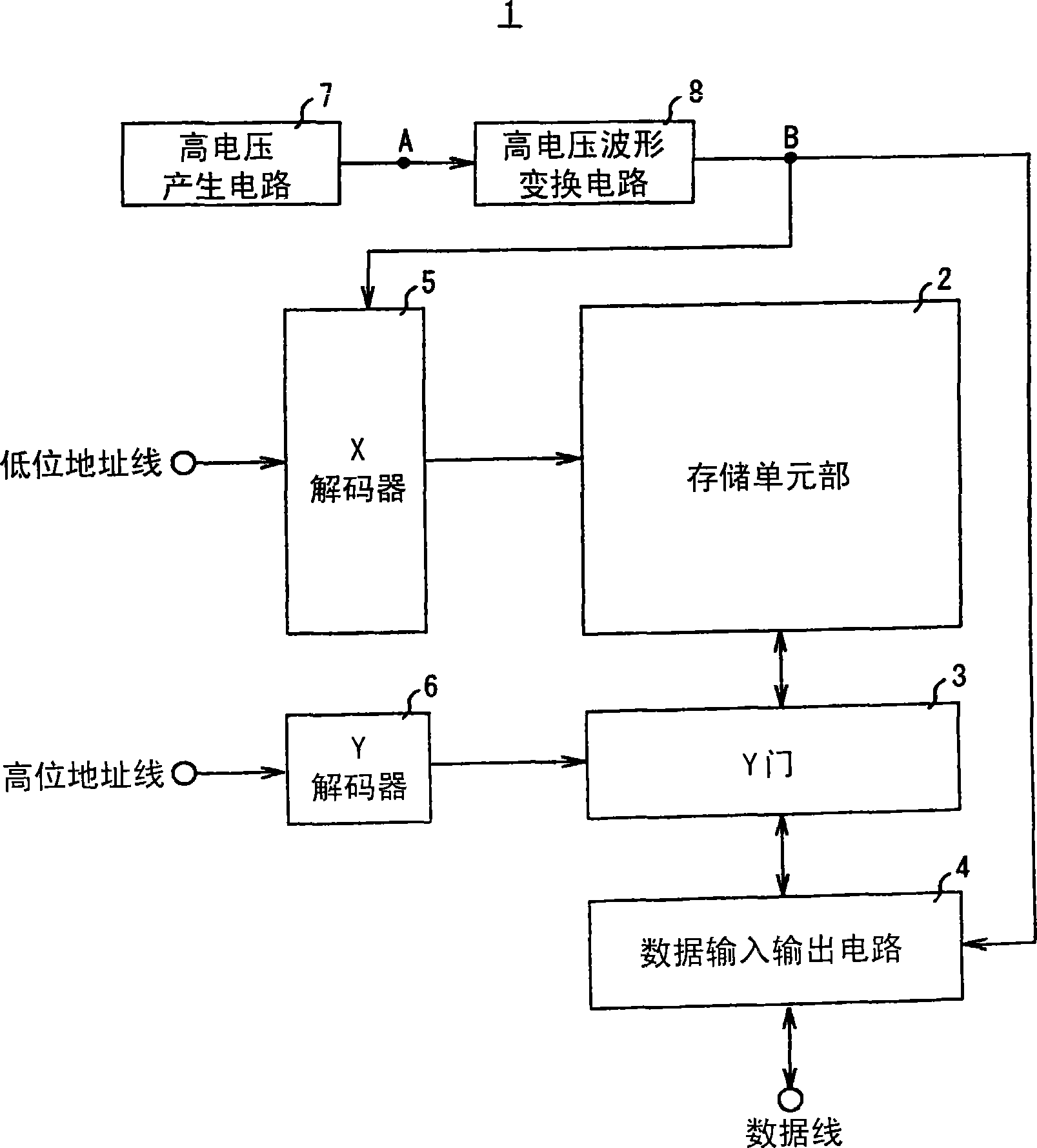
[0026] Hereinafter, preferred embodiments of the present invention will be described with reference to the drawings. figure 1 It is a block diagram of an embodiment when the semiconductor device of the present invention is applied to a nonvolatile memory device. This nonvolatile memory device 1 includes, like a conventional nonvolatile memory device: a memory cell unit 2 provided with a plurality of memory cells; and an X decoder 5 that receives an address signal from a lower address line and selects a memory cell. 1 word line (or control line) of part 2 (not shown in the figure); Y decoder 6, which inputs the address signal of the upper address line, and in the memory cell connected to 1 word line (or control line) Select a fixed memory cell for reading or rewriting; Y gate 3, input the output signal of Y decoder 6, and connect the above-mentioned selected memory cell with data input and output circuit 4; data input and output circuit 4, read out the data of the storage uni...


PUM


Abstract

There is provided a non-volatile memory device capable of improving screening test accuracy while applying voltage below the limit voltage of a high-voltage element in the screening test. The non-volatile memory device (51) includes: a high-voltage generation circuit (7) for generating a high voltage; a high-voltage waveform conversion circuit (58) for inputting the high voltage and converting the voltage waveform; and a memory cell unit (2) for performing data rewrite by applying the converted high voltage. The high-voltage waveform conversion circuit (58) has a test signal input unit TEST. When a test signal is inputted to this test signal input unit, a high voltage inputted from the high-voltage generation circuit (7) is applied to the memory cell unit (2) without converting the voltage waveform.

Description

technical field [0001] The present invention relates to a semiconductor device suitable for use in a nonvolatile memory device such as an EEPROM or a flash memory in which data can be rewritten by applying a high voltage to a memory cell. Background technique [0002] In recent years, EEPROM or flash memory has been widely used to store various programs or store various data in consumer equipment, industrial equipment, and the like. A memory cell constituting an EEPROM or a flash memory injects electrons into a floating gate or releases electrons from the floating gate using tunnel current or hot electrons generated by a high voltage (eg, 15V). As a result, data can be rewritten by changing the threshold value of the memory cell. [0003] In general, semiconductor devices manufactured in a semiconductor factory are subjected to a so-called screening test to remove products that may become defective after shipment with defects. This screening test is performed under conditi...

Claims


Application Information

Patent Timeline
Patent Type & Authority Applications(China)
IPC IPC(8): G11C29/00G11C16/06G11C29/12
CPCG11C29/12G11C16/04G11C29/12005G11C16/06G11C29/00
Inventor 真砂纪之多田佳广
Owner ROHM CO LTD
Features
  • Generate Ideas
  • Intellectual Property
  • Life Sciences
  • Materials
  • Tech Scout
  • Unparalleled Data Quality
  • Higher Quality Content
  • 60% Fewer Hallucinations
Learn More