Solid state image pickup device and camera using the same

A technology of solid-state imaging devices and pixel parts, which is applied to electrical components, image communication, and color TV components, etc., which can solve the problems of increased chip area and cost, and achieve low power consumption, improved linearity, and reduced noise.

Active Publication Date: 2007-02-07
GK BRIDGE 1
View PDF1 Cites 8 Cited by
  • Summary
  • Abstract
  • Description
  • Claims
  • Application Information

AI Technical Summary

Problems solved by technology

In order to prevent this reduction, it is possible to increase the noise canceling capacitors C41 and C42, especially the capacitor C41, but this method leads to an increase in chip area, which becomes a direct cause of cost increase

Method used


Image

  • Solid state image pickup device and camera using the same
  • Solid state image pickup device and camera using the same
  • Solid state image pickup device and camera using the same

Examples


Embodiment approach 1

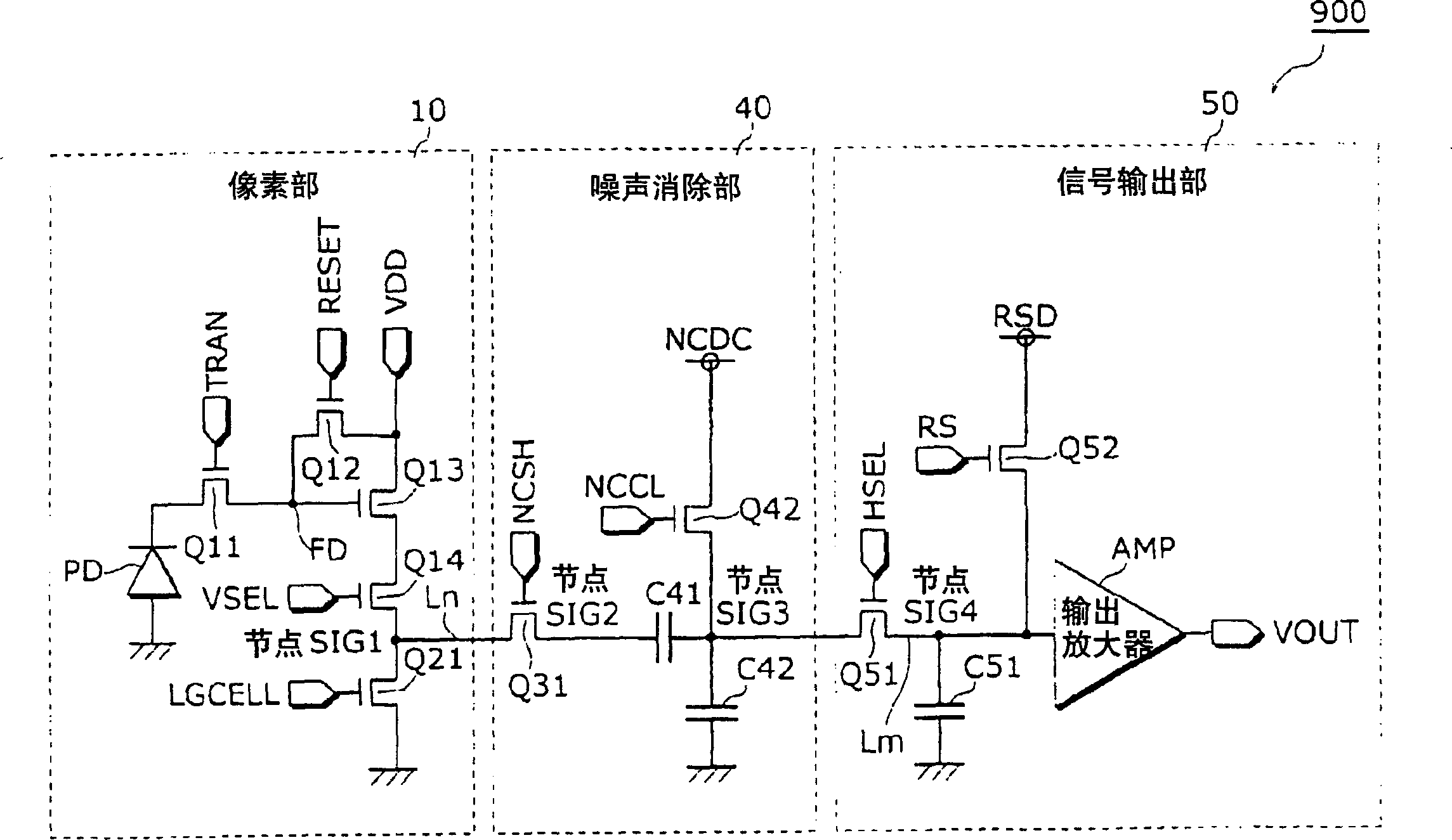
[0119] image 3 It is a schematic circuit diagram of a circuit composed only of N-type MOSs in Embodiment 1 of the present invention, which prevents deterioration of pixel characteristics due to heat treatment in the P-type MOS formation process. where, in this figure, for the figure 1 Components corresponding to the illustrated solid-state imaging device 900 are assigned the same reference numerals, and detailed description thereof will be omitted.

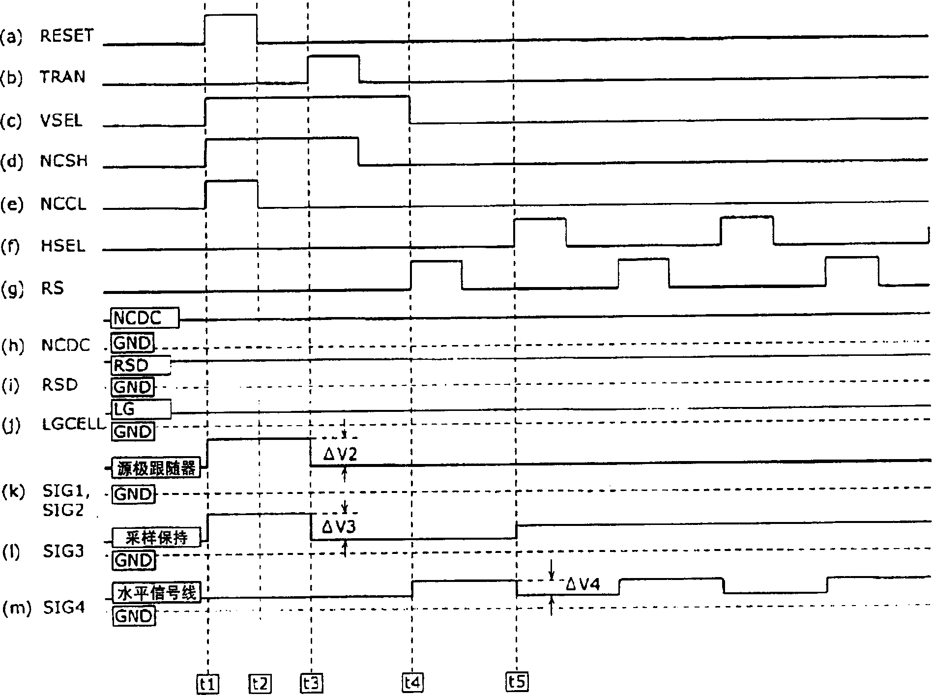
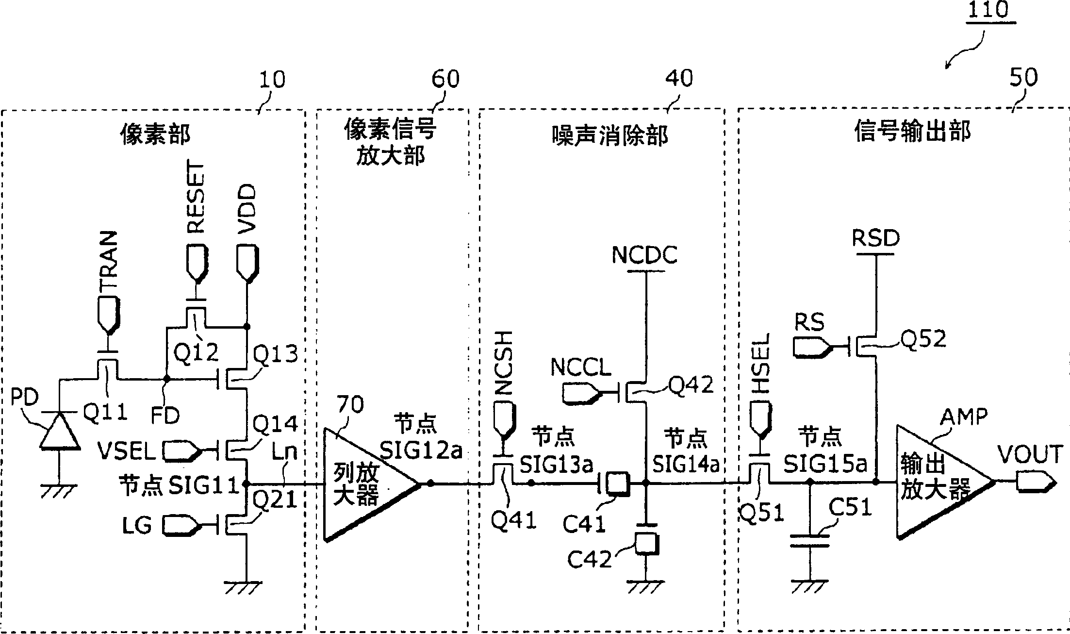
[0120] The solid-state imaging device 110 has a configuration in which a pixel signal amplifying section 60 (that is, a column amplifier 70 ) is inserted between the pixel section 10 and the noise canceling section 40 . Among them, its driving timing and figure 2 Same as shown.

[0121] That is, it becomes the following structure. At time t1, the RESET pulse is turned ON, and VDD is supplied to the floating propagation region FD. At this time, the VSEL pulse is turned ON, and the signal ( image 3 The node SIG11) is provid...

Embodiment approach 2

[0137] Figure 6 A circuit of an NMOS solid-state imaging device according to Embodiment 2 of the present invention in which deterioration of pixel characteristics due to heat treatment in a P-type MOS formation process is prevented is shown. The solid-state imaging device 130 according to Embodiment 2 of the present invention differs from Embodiment 1 in that a source follower circuit for impedance conversion is added to the input portion of the signal output portion 50 a.

[0138] In Embodiment 2, in the circuit of Embodiment 1, the signal from the noise canceling unit 40 is transmitted to the horizontal signal line after first passing through the circuit for performing impedance conversion. Therefore, capacitance distribution due to parasitic capacitance of the horizontal signal line does not occur, and can be compared to The circuit of Embodiment 1 further improves sensitivity and reduces noise, and can also easily reduce the chip area.

[0139] Figure 7 is a driving ti...

Embodiment approach 3

[0147] Figure 8 It is a schematic circuit diagram of an NMOS solid-state imaging device that prevents deterioration of pixel characteristics due to heat treatment in a P-type MOS forming process according to Embodiment 3 of the present invention.

[0148] The solid-state imaging device 140 employs a configuration in which the pixel signal amplifier 60 b can change the amplification factor according to the level of the output voltage of the pixel unit 10 . In this configuration example, the pixel signal amplifying section 60b includes column amplifiers 70a and 70b with different amplification factors selected by the comparator COMP, and the column amplifiers are selected according to the level of the output voltage of the pixel section 10. One of 70a and 70b.

[0149] Comparing the potential of the node SIG61 and VREF in the pixel unit 10 with the comparator COMP, and controlling based on the output potential of the comparator COMP so that when the potential of the node SIG61...


PUM


Abstract

A solid state image pickup device 110 is provided with: a plurality of pixel units 10 that are arranged two-dimensionally and include a photoelectric conversion unit (photodiode PD) that converts light into a charge and an amplification unit (amplifier Q13) that converts the charge into a voltage and outputs it; a plurality of noise signal removal units (noise cancellation units 40) that are provided one for each column and remove noises contained in the voltage outputted from the amplifier Q31 of the pixel unit 10 belonging to the column; and a plurality of column amplification units (column amplifiers 70) that amplify the voltage outputted from the amplifier Q13 of the pixel unit 10 and output the amplified voltage to the noise cancellation unit 40, and enables increase in sensitivity and reduction in noise with low power consumption.

Description

technical field [0001] The present invention relates to a solid-state imaging device and a video camera using the same, and particularly relates to a technology capable of improving sensitivity and reducing noise with low power consumption. Background technique [0002] figure 1 It is a circuit diagram of a conventional solid-state imaging device 900 composed only of N-type MOS. [0003] exist figure 1 The illustrated solid-state imaging device 900 employs a configuration in which incident light is converted into a voltage by the pixel unit 10 , voltage variations between pixels are reduced by the noise canceller 40 , and voltages are sequentially output by the signal output unit 50 . [0004] In more detail, as figure 1 As shown, the solid-state imaging device 900 includes a plurality of (one in the figure) pixel units 10 arranged two-dimensionally, a plurality of (one in the figure in the figure) noise canceling units 40 provided for each column, and a signal output uni...

Claims


Application Information

Patent Timeline
Patent Type & Authority Applications(China)
IPC IPC(8): H04N5/335H01L27/146H04N5/357H04N5/378
CPCH04N5/378H04N5/357H04N25/60H04N25/75
Inventor 春日繁孝山口琢己村田隆彦松长诚之宫川良平植田敦
Owner GK BRIDGE 1
Why Eureka
Try Eureka