Photoresist stripping method
A technology of photoresist and photoresist layer, which is applied in optics, photosensitive material processing, original parts for opto-mechanical processing, etc. Remove metal oxides and other problems to avoid metal oxides, reduce resistance, and improve device performance
- Summary
- Abstract
- Description
- Claims
- Application Information
AI Technical Summary
Problems solved by technology
Method used
Image

Examples
Embodiment Construction
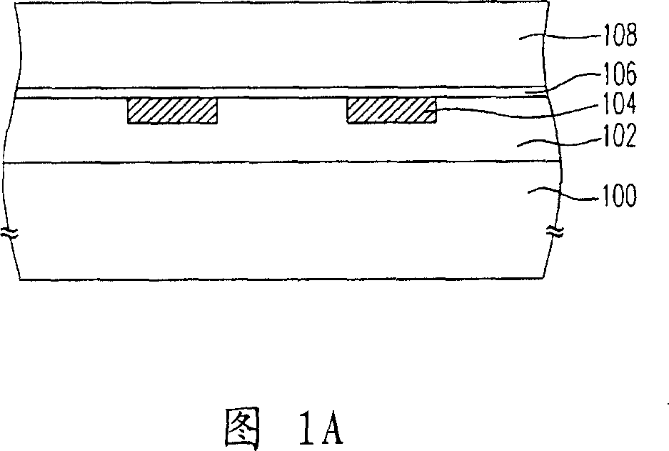
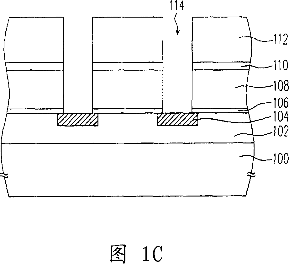
[0034] 1A to 1D are cross-sectional views illustrating a manufacturing process of a contact window opening according to a preferred embodiment of the present invention. Referring to FIG. 1 , firstly, a dielectric layer 102 is formed on a semiconductor substrate 100 , and a plurality of contact structures 104 are formed in the dielectric layer 102 . Wherein, the material of the contact structure 104 is, for example, nickel silicide (siliconnitride) or an alloy containing nickel silicide, and the alloy of nickel silicide is, for example, platinum or palladium.
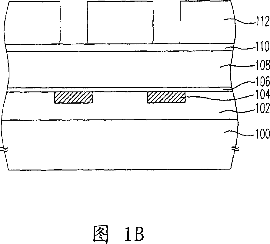
[0035] Next, please continue to refer to FIG. 1A, a barrier layer (barrier layer) 106 is formed on the dielectric layer 102, and its material is, for example, silicon nitride (silicon nitride), and the formation method is, for example, chemical vapor deposition (chemical vapor deposition, CVD). Then, a dielectric layer 108 is formed on the barrier layer 106, and its material is, for example, silicon oxide, and its formi...
PUM
 Abstract
Description
Claims
Application Information
 - R&D
- Intellectual Property
- Life Sciences
- Materials
- Tech Scout
- Unparalleled Data Quality
- Higher Quality Content
- 60% Fewer Hallucinations
Browse by: Latest US Patents, China's latest patents, Technical Efficacy Thesaurus, Application Domain, Technology Topic, Popular Technical Reports.
© 2025 PatSnap. All rights reserved.Legal|Privacy policy|Modern Slavery Act Transparency Statement|Sitemap|About US| Contact US: help@patsnap.com