Low-temperature chip direct bonding method

A wafer bonding and wafer technology, applied in electrical components, semiconductor/solid-state device manufacturing, circuits, etc., which can solve problems such as advanced experimental conditions and high environmental dependence, stress and debonding problems that cannot be ignored, etc.

Inactive Publication Date: 2007-03-21
INST OF SEMICONDUCTORS - CHINESE ACAD OF SCI
View PDF0 Cites 18 Cited by
  • Summary
  • Abstract
  • Description
  • Claims
  • Application Information

AI Technical Summary

Problems solved by technology

[0003] To sum up, some researchers have carried out bonding experiments at high temperature and achieved some results, but the stress and debonding problems caused by the difference in thermal expansion coefficient of bonding at high temperature are still not to be ignored.
There are al

Method used


Image

  • Low-temperature chip direct bonding method
  • Low-temperature chip direct bonding method
  • Low-temperature chip direct bonding method

Examples


Embodiment Construction

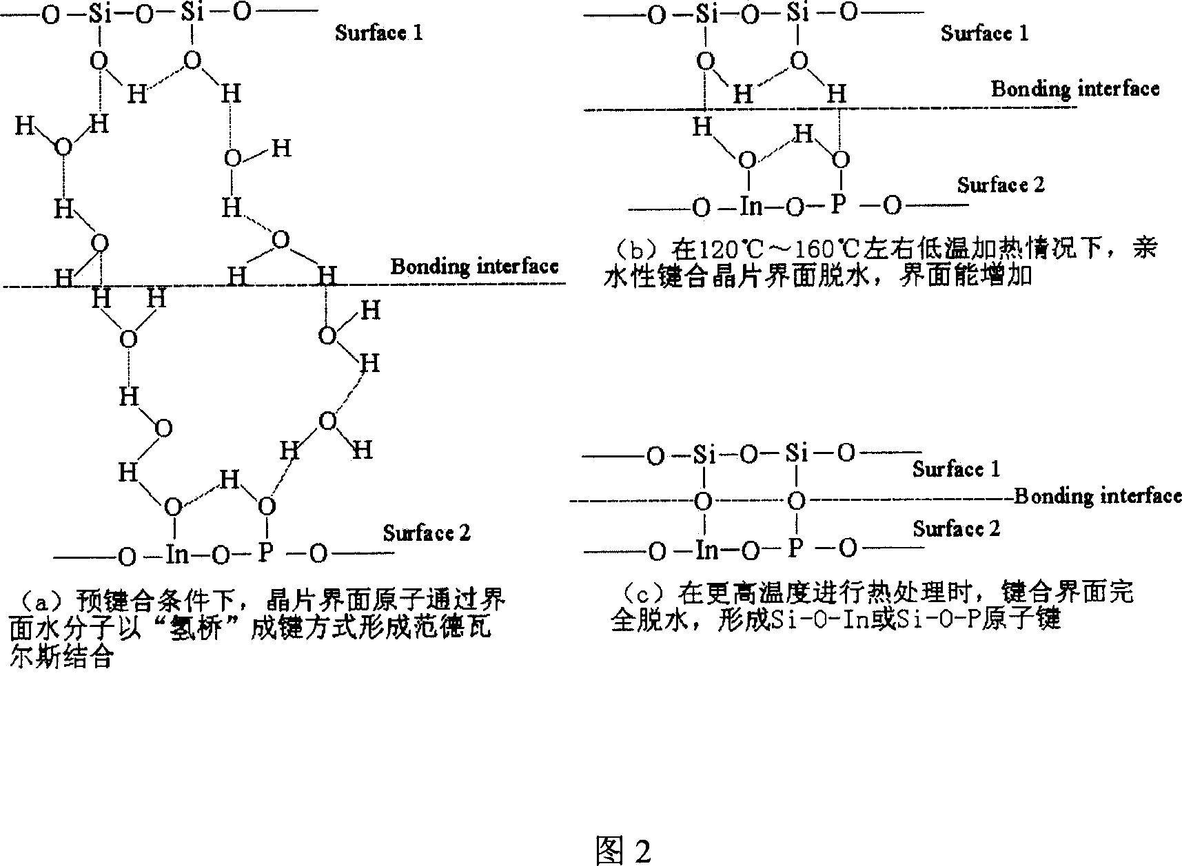
[0039] The InP-based wafer and the p-type Si wafer with the quantum well epitaxial structure in Fig. 1 are bonded together after the cleaning process, and then the bonding energy is improved through the above-mentioned thinning and heating process. The InP substrate is subsequently etched away by wet etching.

[0040] Figure 2(a) shows the "hydrogen bridge" van der Waals bonding formed by water molecules between the wafer interfaces in the case of low temperature (below 100°C) pre-bonding; (b) shows that when the temperature rises to about 120-160°C At this time, the interface water molecules are partially evaporated to form a short-range combination of water molecules. At this time, the interface surface energy is enough to thin the wafer; (c) shows that the bonded sheet is subjected to a higher temperature at a temperature above 200 ° C. During processing, the interfacial water molecules escape completely and the interface begins to form covalent bonds.

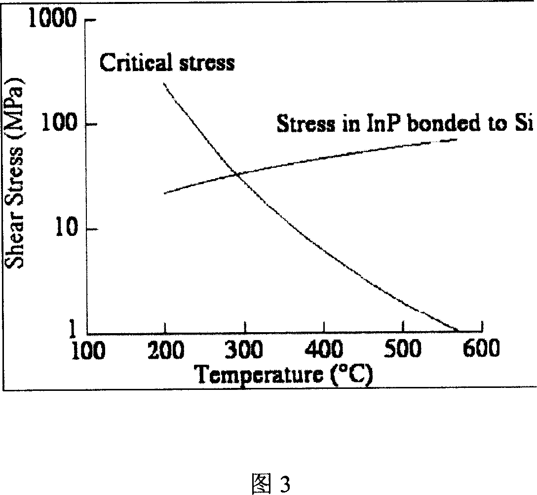
[0041] Figure 3 is...


PUM


Abstract

A method relates to wafer straight bonding technology field and uses low temperature bonding technology to bond InP group stuff on Si surface. Remove one layer hydrophobic organic on surface of single polishing Si and InP wafers by organic solvent, remove impurity ion and carbon and surface rinsing dispose to them, then carry the pretreatment. Put the pretreatment wafers into one vacuum furnace system with temperature controller to adding temperature and pressure, then carry heating dispose with proper temperature and pressure to remove hydrosphere of bonding surface. Carry thinner dispose for bonding piece and heat treatment of removing left gas to surface without pressure to make heat treatment at higher temperature for enhance surface bonding ability. At last, carry InP underlay cauterization with bonding piece. It uses for micro-electronics and silicon-base photoelectron field.

Description

technical field [0001] The invention relates to the technical field of wafer bonding, in particular to a low-temperature wafer bonding method. Background technique [0002] With the increasing application of III-V semiconductor materials, the bonding of III-V semiconductor materials and Si by wafer bonding method has attracted more and more people's interest. The bonding of Si with InP and GaAs materials with lattice mismatch and large thermal expansion coefficient mismatch to prepare Si-based long-wavelength lasers or photonic crystals has been reported earlier. Hiroshi Wada et al. used the lift-off method to realize the bonding of InP-based long-wavelength vertical cavity surface emitting lasers on Si and successfully lased them, "Room-Temperature Photo-Pumped Operation of 1.58-μmVertical-Cavity Lasers Fabricated on Si Substrates Using Wafer Bonding," IEEE PHOTONICS TECHNOLOGY LETTERS, Vol. 8: 11, pp. 1426-1428 (1996). Shinpei Ogawa and others realized the bonding of InP...

Claims


Application Information

Patent Timeline
IPC IPC(8): H01L21/00
Inventor 赵洪泉于丽娟黄永箴
Owner INST OF SEMICONDUCTORS - CHINESE ACAD OF SCI
Why Eureka
Try Eureka