Bipolar semiconductor device and process for producing the same

A manufacturing method, semiconductor technology, applied in the direction of semiconductor/solid-state device manufacturing, semiconductor devices, transistors, etc., can solve the problems of increased component loss, increased power conversion device loss, and reduced reliability, and achieve the effect of reducing transmission

Inactive Publication Date: 2007-03-28
THE KANSAI ELECTRIC POWER CO +1
View PDF1 Cites 10 Cited by
  • Summary
  • Abstract
  • Description
  • Claims
  • Application Information

AI Technical Summary

Problems solved by technology

An increase in the forward voltage will increase the loss of the element, so it will increase the loss of power conversion devices such as inverters using this element, and cause a decrease in reliability

Method used


Image

  • Bipolar semiconductor device and process for producing the same
  • Bipolar semiconductor device and process for producing the same
  • Bipolar semiconductor device and process for producing the same

Examples


Embodiment 1

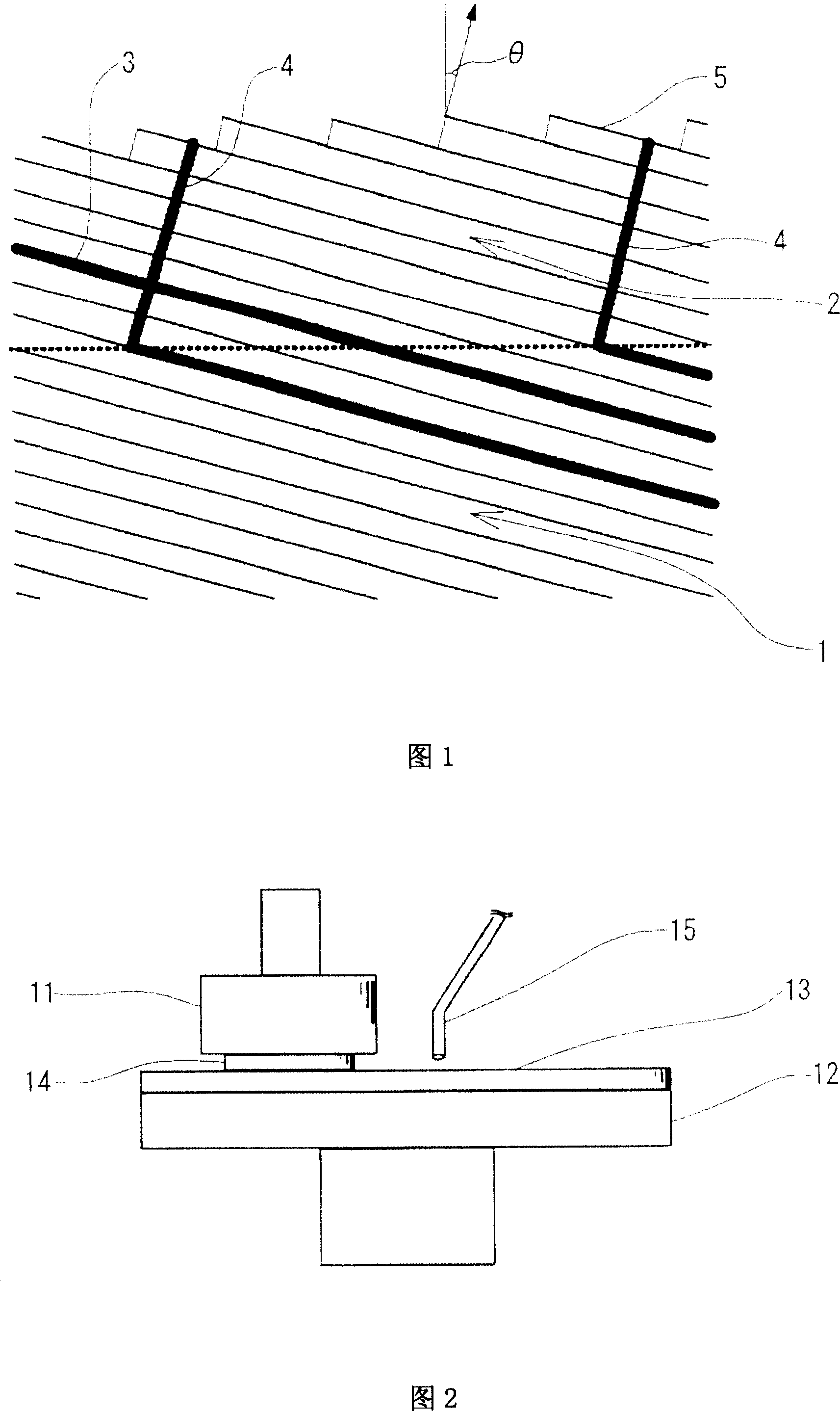
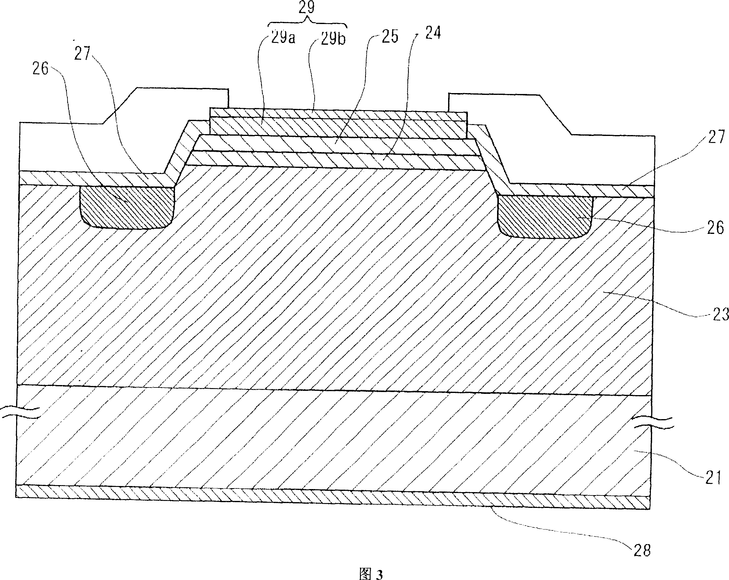
[0097] Using a vertical thermal furnace, the crystal block grown by the modified Rayleigh method is cut into thin slices according to the oblique orientation [11-20] and the deviation angle is 8°, and the mirror-like n-type 4H- For the SiC (0001) substrate, hydrogen gas was supplied to the substrate at a flow rate of 10 L / min, and etching treatment was performed at a temperature of 1400° C. and a pressure of 30 Torr for 40 minutes. The surface roughness Rms of the treated substrate surface was measured with an atomic force microscope SPI3800N manufactured by Seiko Instruments Co., Ltd. and found to be 0.25 nm (area of ​​10 μm×10 μm).

[0098] Second, epitaxially grow silicon carbide on the surface of the treated substrate by CVD. While supplying propane (8cc / min), silane (30cc / min), and hydrogen (10L / min), at a temperature of 1545°C and a pressure of 42Torr, a stepwise slip growth was performed for 4 hours to form a film with a thickness of 60μm. epitaxial film.

[0099] For...

Embodiment 2

[0101] A silicon carbide single crystal substrate with an epitaxial film was obtained in the same manner as in Example 1 except that the surface of the substrate was treated by chemical mechanical polishing before the hydrogen etching treatment. The surface roughness Rms of the treated substrate surface was measured in the same manner as in Example 1 and found to be 0.20 nm (area of ​​10 μm×10 μm).

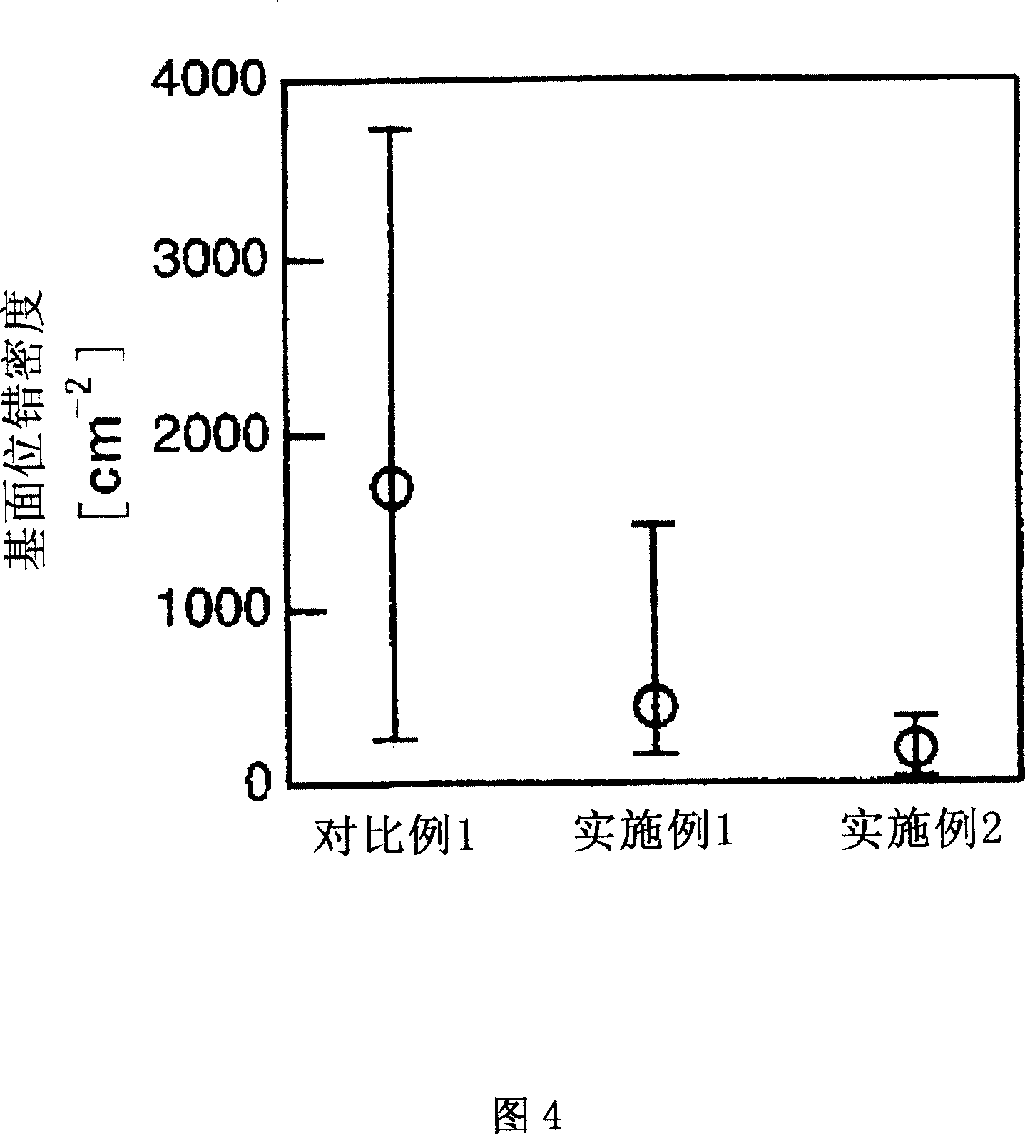
[0102] For the obtained silicon carbide single crystal substrate with epitaxial film, the results of measuring the basal plane dislocation density in the epitaxial film by using molten KOH corrosion and X-ray topography, the average value is 60cm -2 .

Embodiment 3

[0104] A mirror-like n-type 4H-SiC (000-1) obtained by cutting the crystal block grown by the modified Rayleigh method into thin slices with an oblique orientation [11-20] and an off-angle of 8°, and mechanically grinding the surface with abrasive grains The substrate was subjected to the same chemical mechanical polishing treatment and hydrogen etching treatment as in Example 2 to grow an epitaxial film. In the same manner as in Example 1, the surface roughness Rms of the treated substrate surface was measured to be 0.20 nm (area of ​​10 μm×10 μm).

[0105] For the obtained silicon carbide single crystal substrate with epitaxial film, the results of measuring the basal plane dislocation density in the epitaxial film by using molten KOH corrosion and X-ray topography, the average value is 20 cm -2 .


PUM

PropertyMeasurementUnit
thicknessaaaaaaaaaa
thicknessaaaaaaaaaa
thicknessaaaaaaaaaa

Abstract

Production of a bipolar semiconductor device having at least part of a region wherein at current passage electrons and holes re-couple with each other formed of an epitaxial layer of silicon carbide grown from a surface of silicon carbide substrate, wherein the epitaxial layer is formed by first performing hydrogen etching of a surface of silicon carbide substrate and thereafter effecting epitaxial growth of silicon carbide from the etched surface. Further propagation of a basal plane dislocation to the epitaxial layer can be reduced by subjecting the surface of silicon carbide substrate to chemical mechanical polishing prior to the hydrogen etching.

Description

technical field [0001] The invention relates to a semiconductor device and a manufacturing method thereof which form a drift layer and other regions where electrons and holes recombine when energized through a silicon carbide epitaxial layer grown on the surface of a silicon carbide substrate. In particular, it relates to the reduction of the basal plane dislocation density in the epitaxial layer, and the improvement of the forward voltage degradation over time. Background technique [0002] The dielectric breakdown electric field strength of silicon carbide (SiC) is about 10 times that of silicon (Si). In other aspects such as thermal conductivity, electron mobility, band gap, etc., silicon carbide is also a semiconductor with excellent physical properties. Therefore, compared with the existing silicon-based power semiconductor components, silicon carbide is expected to become a semiconductor material with greatly improved performance. Recently, single crystal substrates ...

Claims


Application Information

Patent Timeline
Patent Type & Authority Applications(China)
IPC IPC(8): H01L21/20H01L21/205H01L21/302H01L21/331H01L21/336H01L29/73H01L29/74H01L29/78H01L29/861H01L21/04H01L29/737
CPCH01L21/02019H01L21/2053H01L21/02024H01L29/8613H01L21/02378H01L21/02433H01L21/02529H01L21/0262H01L21/02661
Inventor 中山浩二菅原良孝土田秀一镰田功穗三柳俊之中村智宣
Owner THE KANSAI ELECTRIC POWER CO
Why Eureka
Try Eureka