Semiconductor light-emitting device

A technology of light-emitting elements and semiconductors, applied in semiconductor devices, electrical components, circuits, etc., can solve problems such as reduced component life, increased tunnel voltage, and dopant diffusion

Inactive Publication Date: 2007-04-04
HITACHI CABLE
View PDF1 Cites 18 Cited by
  • Summary
  • Abstract
  • Description
  • Claims
  • Application Information

AI Technical Summary

Problems solved by technology

[0008] However, it is necessary to form the contact layer as a high carrier concentration layer and be a thin film because the contact layer must provide a tunnel junction and be a light absorbing layer for light emitted from the active layer, and due to the heat generated during growth, It is easy to cause the diffusion of dopants, which leads to the following two problems
[0009] First, the dopant diffuses from the contact layer to the depth direction of the LED element, diffuses into the active layer of the LED element, and causes defects in the active layer. These defects act as non-luminescent recombination components, resulting in a decrease in the light output of the LED element
[0010] Second, due to the diffusion of p-type dopants, the actual carrier concentration of the contact layer of the high-carrier concentration layer as a thin film decreases, so it is difficult to complete the above-mentioned tunnel junction, resulting in an increase in the tunnel voltage, and the LED element Drive voltage (forward voltage) rises harmfully
[0017] However, the only problem in the case of using Zn and Mg in combination is the above-mentioned interdiffusion between Zn and Mg, and it is necessary to suppress the decrease in device life caused by this.
[0018] On the other hand, there is also such a method, that is, a contact layer is directly arranged on the p-type cladding layer without a buffer layer, and an ITO film is arranged on it (for example, U.S. Patent No. 35665). solution, since the film thickness of the p-type cladding layer is thin, the diffusion of dopants is easy to reach the active layer, so the device life of the above structure is easy to decrease
Also, since the film thickness of the p-type cladding layer is thin, the element is easily damaged when connecting wires

Method used


Image

  • Semiconductor light-emitting device
  • Semiconductor light-emitting device
  • Semiconductor light-emitting device

Examples


no. 1 approach

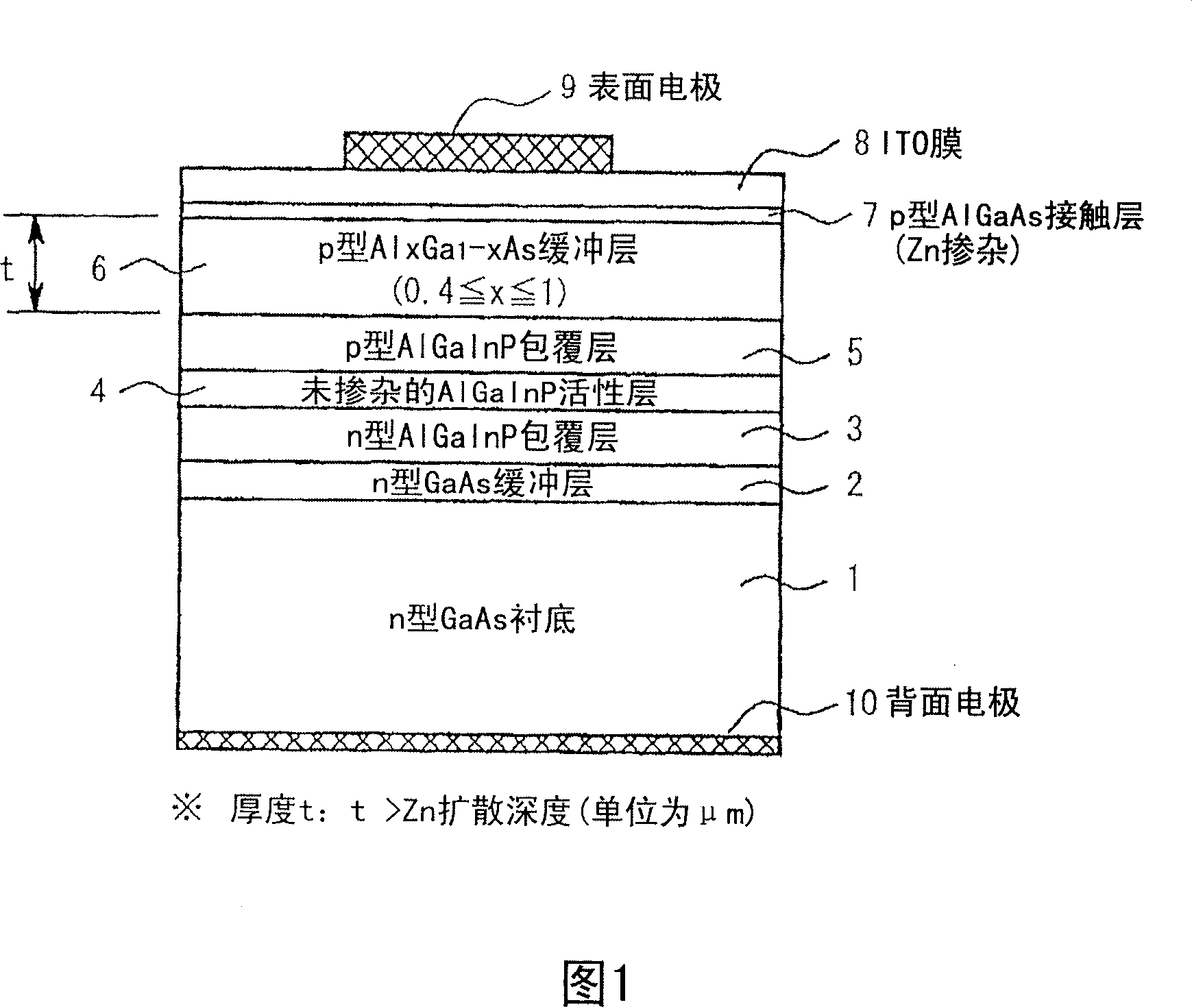
[0081] FIG. 1 is a cross-sectional view showing an AlGaInP-based red LED according to a first preferred embodiment of the present invention.

[0082] The LED comprises the following layers formed sequentially on an n-type GaAs substrate 1 as a semiconductor substrate: n-type GaAs buffer layer 2, n-type AlGaInP cladding layer 3 (abbreviated as n-type cladding layer), undoped The AlGaInP active layer 4 (referred to as the active layer for short), and the p-type AlGaInP cladding layer 5 (referred to as the p-type cladding layer for short), wherein, 3-5 layers are epitaxially grown to form the light emitting part. Furthermore, an As-based p-type AlGaAs contact layer 7 (abbreviated as a p-type contact layer) to which a p-type dopant is added at a high concentration is formed on the p-type cladding layer 5 . On the p-type contact layer 7, an ITO film 8 (current spreading layer) as a transparent conductive film is formed as a current spreading layer made of a metal oxide, and a surfa...

Embodiment 1

[0123] In Example 1, an epitaxial growth wafer for a red LED having an emission wavelength around 630 nm and having the structure shown in FIG. 1 was produced. The growth method of the epitaxial growth, the film thickness of the epitaxial growth layer, the structure of the epitaxial layer, the formation method of the electrode, and the manufacturing method of the LED element are as follows.

[0124] Using the MOVPE method, on the n-type GaAs substrate 1 with Si as the dopant, the layers are sequentially grown: n-type (Si-doped) GaAs buffer layer 2 (film thickness 200nm, carrier concentration 1×10 18 / cm 3 ), n-type (Si-doped) (Al 0.7 Ga 0.3 ) 0.5 In 0.5 P cladding layer 3 (film thickness 400nm, carrier concentration 1×10 18 / cm 3 ), undoped (Al0.1 Ga 0.9 ) 0.5 In 0.5 P active layer 4 (film thickness 600nm), p-type (Mg-doped) (Al 0.7 Ga 0.3 ) 0.5 In 0.5 P cladding layer 5 (film thickness 400nm, carrier concentration 1.2×10 18 / cm 3 ), p-type (Mg-doped) (Al 0.85 ...

Embodiment 2

[0141] In Example 2, an epitaxial growth wafer for a red LED having an emission wavelength around 630 nm and having the structure shown in FIG. 3 was produced. The growth method of the epitaxial growth, the film thickness of the epitaxial growth layer, the structure of the epitaxial layer, the method of forming the electrodes, and the manufacturing method of the LED element are basically the same as those of the above-mentioned Example 1 (FIG. 1). Differences from Example 1 are enumerated below and described in detail.

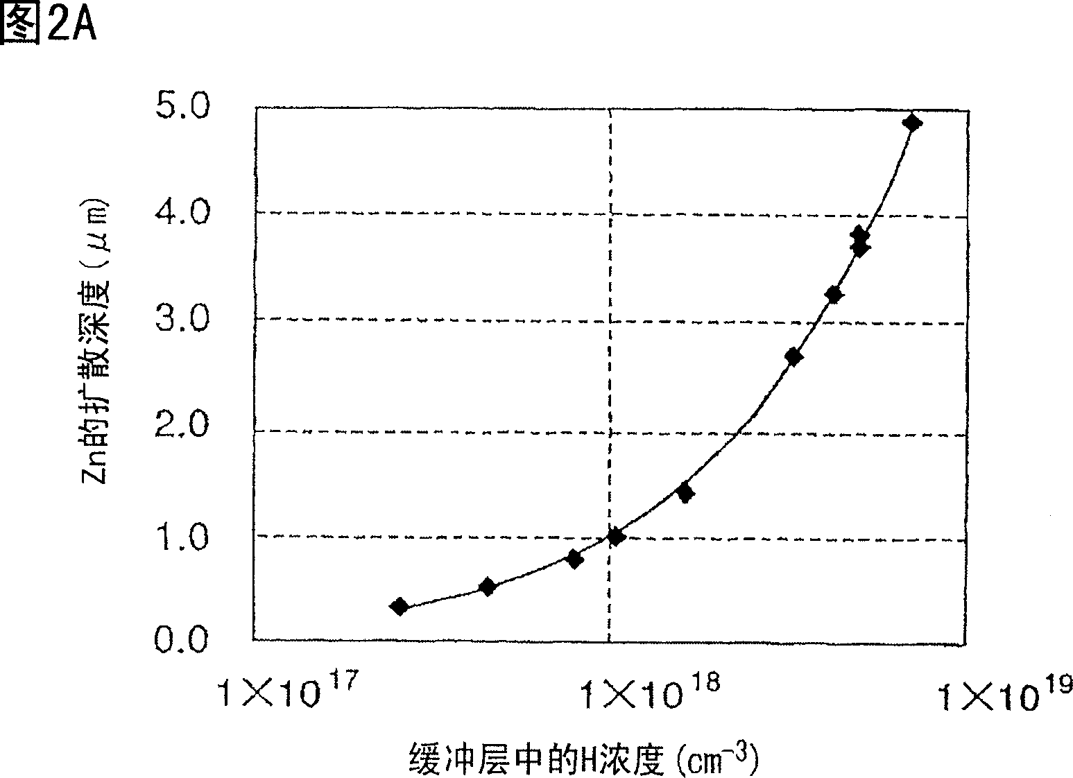
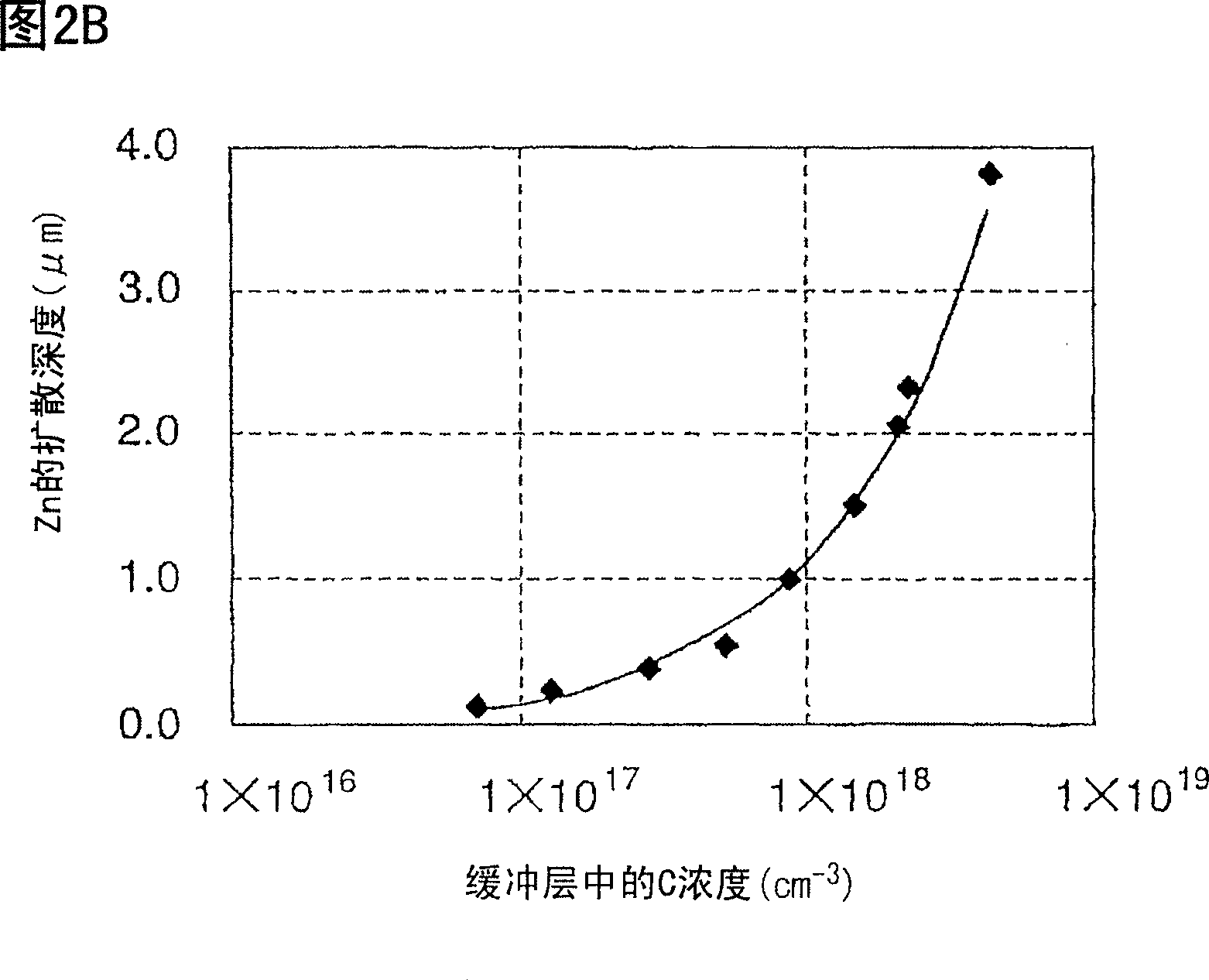
[0142] In Example 2, a diffusion preventing layer 11 is provided between the active layer 4 and the p-type cladding layer 5, and this layer is a semiconductor layer not positively added, that is, a so-called undoped layer. The diffusion prevention layer 11 prevents the p-type dopant diffused from the p-type semiconductor layer including the above-mentioned p-type cladding layer 5 and the upper layer from being mixed into the active layer 4 . The composition o...


PUM


Abstract

A semiconductor light emitting device comprises: a light-emitting portion formed on a semiconductor substrate, an As-based p-type contact layer formed thereon, a current spreading layer formed thereon of a metal oxide material, and a buffer layer formed between the p-type cladding layer and the p-type contact layer. The buffer layer has a group III/V semiconductor with a p-type conductivity and hydrogen or carbon included intentionally or unavoidably therein, and the buffer layer has a thickness equal to or greater than a diffusion length L of a dopant doped into the p-type contact layer.

Description

technical field [0001] The invention relates to a semiconductor light-emitting element, more specifically, the invention relates to a high-brightness semiconductor light-emitting element with a transparent conductive film as a current spreading layer. Background technique [0002] In the past, light-emitting diodes (hereinafter referred to as LEDs), which were used as semiconductor light-emitting elements, have grown GaN-based and AlGaInP-based high-quality crystals by using the MOVPE method in recent years, so blue, green, orange, yellow, and red high-brightness crystals can be produced. LED. [0003] However, in order to obtain high luminance, good current spreading characteristics are required to uniformly supply current to the chip surface of the LED. For example, in an AlGaInP-based LED element, the film thickness of the current spreading layer needs to be about 5 to 10 μm. Therefore, the cost of raw materials consumed in the growth of the current spreading layer is in...

Claims


Application Information

Patent Timeline
Patent Type & Authority Applications(China)
IPC IPC(8): H01L33/00H01L33/06H01L33/12H01L33/30H01L33/42
Inventor 新井优洋今野泰一郎饭塚和幸秋元克弥
Owner HITACHI CABLE
Why Eureka
Try Eureka