Supercharge Your Innovation With Domain-Expert AI Agents!

TFT LCD array substrate structure and its producing method

An array substrate structure and substrate technology, which are used in semiconductor/solid-state device manufacturing, semiconductor/solid-state device components, instruments, etc., can solve problems such as the failure of the common electrode to load the common voltage, the failure of the common electrode line, and the poor bright line, etc. The effect of reducing common electrode defects, improving yield, and increasing storage capacitance

Active Publication Date: 2007-04-11
K TRONICS (SUZHOU) TECH CO LTD +1
View PDF0 Cites 5 Cited by
  • Summary
  • Abstract
  • Description
  • Claims
  • Application Information

AI Technical Summary

Problems solved by technology

[0011] Fig. 4 is a schematic diagram of the structure of the common electrode of the gate metal layer in the prior art. As long as one defect occurs on the common electrode line of the gate metal layer of this structure, the common voltage on the common electrode cannot be applied, resulting in the failure of the entire line. The failure of the common electrode wire leads to poor bright lines, and it is difficult to repair

Method used


Image

  • TFT LCD array substrate structure and its producing method
  • TFT LCD array substrate structure and its producing method
  • TFT LCD array substrate structure and its producing method

Examples


Embodiment Construction

[0052] The present invention will be further described in detail below in conjunction with the description of the accompanying drawings and preferred specific embodiments.

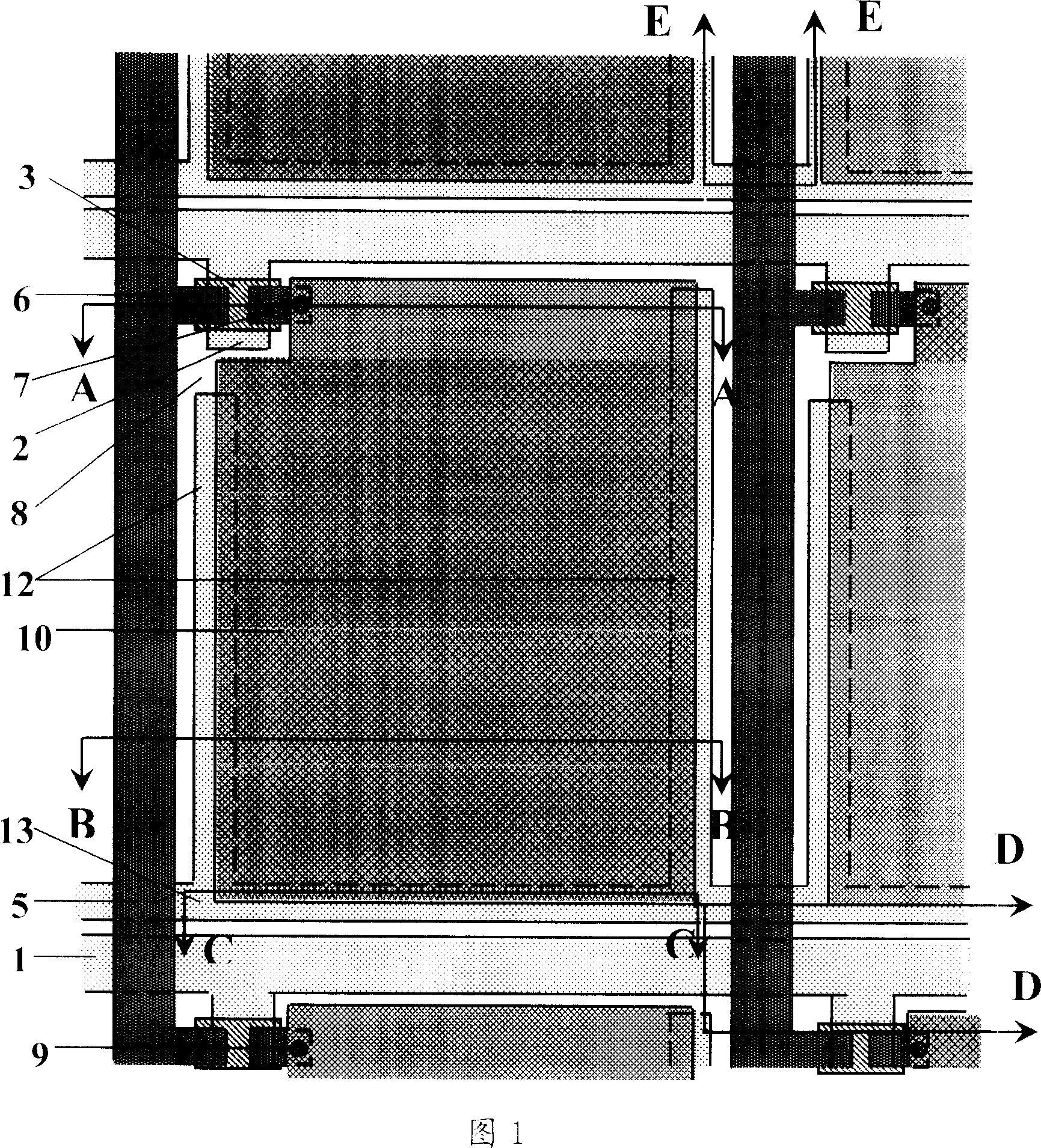
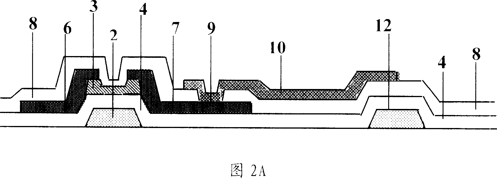
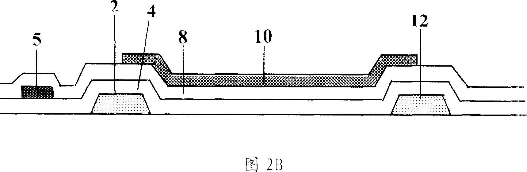
[0053]5 to 6E are schematic structural diagrams of the TFT LCD array substrate of the present invention. As shown in Figure 5, on the array substrate of the TFT LCD, there are a group of gate scanning lines 1, a signal metal layer common electrode 15 parallel to the gate scanning lines 1, and a group of data scanning lines 5 and signal metal layer perpendicular to it. Layer light blocking strip 14. Adjacent gate scan lines 1 and data scan lines 5 define pixel regions. Each pixel includes a thin film transistor switching device, a transparent pixel electrode 10 , two signal metal layer light blocking strips 14 and part of the signal metal layer common electrode 15 . As shown in FIG. 6A , the thin film transistor switching device is composed of a gate electrode 2 , a gate electrode insulating layer 4 , an ...


PUM


Abstract

This invention discloses a TFT LCD array base plate structure including: a base plate, a grid scanning line and a grid, a grid insulation layer, an active layer, a data scanning line, a source and a drain, light strips and a public electrode, passivation layers formed on the data scanning line, the source and the drain, the light strips and the public electrode, through holes formed on the drain, the light strips and the public electrode, a pixel electrode, a vertical connecting line formed on the passivation layers connecting the light strips vertically by the through hole, a lateral connecting line formed on the passivation layer connecting the public electrodes laterally via the through hole on the public electrode. This invention also discloses a manufacturing method for said TFT LCD array base plate structure.

Description

technical field [0001] The invention relates to a thin film transistor liquid crystal display (TFT LCD), in particular to a thin film transistor liquid crystal display (TFT LCD) array substrate structure and a manufacturing method thereof. Background technique [0002] TFT LCD occupies a dominant position in the current flat panel display market due to its small size, low power consumption, and no radiation. TFT LCD devices are formed by combining array glass substrates and color filter glass substrates. [0003] 1 to 2E are top views and cross-sectional views of various parts of a thin film transistor liquid crystal display array substrate in the prior art. As shown in the figure, the array substrate in the prior art mainly includes: a substrate, a gate scanning line 1 and a gate electrode 2 formed on the substrate; a gate electrode insulating layer 4 and an active layer 3 formed on the gate electrode; The signal scanning line 5, the source electrode 6 and the drain elect...

Claims


Application Information

Patent Timeline
IPC IPC(8): H01L27/12H01L23/522H01L21/84H01L21/768G02F1/136
Inventor 李欣欣李昌熙龙春平
Owner K TRONICS (SUZHOU) TECH CO LTD
Features
  • R&D
  • Intellectual Property
  • Life Sciences
  • Materials
  • Tech Scout
  • Unparalleled Data Quality
  • Higher Quality Content
  • 60% Fewer Hallucinations
Learn More