Method for measuring doping content of semiconductor based on free carrier absorption technique

A technology of carrier absorption and doping concentration, which is applied in the field of semiconductor doping concentration measurement, can solve the problems of inaccurate measurement of doping concentration, difficulty in measurement calibration, and influence on measurement accuracy, and achieve high measurement accuracy and sensitivity, The effect of easy measurement calibration and large measurement range

Inactive Publication Date: 2007-05-30
INST OF OPTICS & ELECTRONICS - CHINESE ACAD OF SCI
View PDF0 Cites 18 Cited by
  • Summary
  • Abstract
  • Description
  • Claims
  • Application Information

AI Technical Summary

Problems solved by technology

[0007] Current industrial use of light-modulated reflection-thermal probe technology in thermal wave method (W.Lee Smith, Allan Rosencwaig, and David L. Willenborg, Ion implant monitoring with thermal wave technology, Appl.Phys.Lett.47, 584-586 (1984)) measure semiconductor doping concentration, mainly used in the measurement of low doping concentration, but thermal probe method has its own shortcoming: a. the doping concentration range of measurement is 10 11 -10 16 cm -2
For lower implantation energy (11 cm -2 ) doped semiconductor, the doping concentration cannot be accurately measured; b. If the doped semiconductor is annealed, the measurement range will be expanded to a certain extent, but the sensitivity will decrease; c. Since the modulated reflection signal detected by the detector is affected by The dual effects of the temperature field and carrier distribution in the semiconductor, the signal amplitude and phase and the doping concentration are not monotonous, but a very complex function, which brings difficulties to the measurement calibration and affects to a certain extent measurement accuracy

Method used


Image

  • Method for measuring doping content of semiconductor based on free carrier absorption technique

Examples


Embodiment Construction

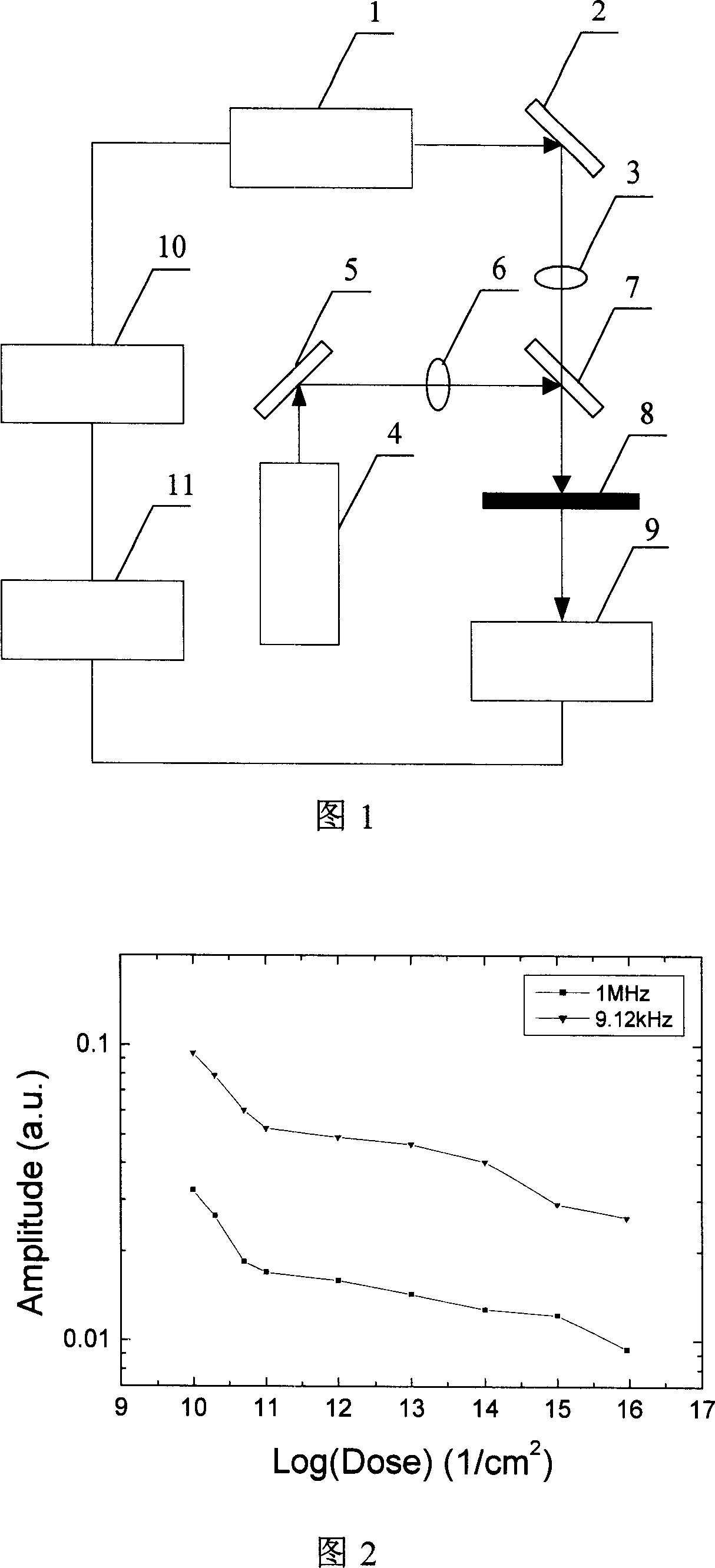
[0019] As shown in Figure 1, the measuring device adopted in the present invention consists of a pump light source 1, a pump light reflector 2, a pump light focus lens 3, a probe light source 4, a probe light reflector 5, a probe light focus lens 6, a two-color beam splitter mirror 7, a semiconductor wafer to be tested 8, a photodetector 9, a function generator 10, and a lock-in amplifier 11. The function generator 10 is connected to the pumping light source 1 to periodically modulate the light intensity of the light source, and is connected to the lock-in amplifier 11 as a reference signal. The signal output by the photodetector 9 is connected to the lock-in amplifier 11 for detection, so as to record the amplitude and phase of the signal.

[0020] The pump light source 1 adopts a modulated semiconductor laser with a central wavelength of 785nm and a power of 95mW, which is modulated by a function generator 8; the detection light source 3 adopts a continuous semiconductor las...


PUM


Abstract

This invention relates to one semiconductor mixture contraction measurement method based on freedom load flow absorption technique, which is characterized by the following: using one beam of photon with energy larger than the continuous laser with light intensity modulation of forbidden band as pump light source; using another beam of light smaller than semiconductor forbidden band width as detector light source; two beams of light are lighting onto same or adjacent positions on semiconductors; the semiconductor absorbs pump light to generate modulation free load flow; due to modulation free load flow absorbing through semiconductor or reflection detector light intensity by lock phase type or reflection detecting light signals for once resonance vibration and phase to get the mixture concentration.

Description

technical field [0001] The invention relates to a method for measuring semiconductor characteristics, in particular to a method for measuring semiconductor doping concentration. Background technique [0002] Doping is the basis for the formation of pn junctions in semiconductor devices, the main means to regulate the electrical properties of semiconductor devices, and a very important link in microelectronics manufacturing technology. The precise control of doping concentration and its uniformity determines to a large extent performance of microelectronic devices. Accurately monitoring the doping concentration of doped semiconductors is a very important topic in semiconductor manufacturing technology. [0003] Judging from the situation of technology novelty search and literature retrieval at home and abroad, the existing semiconductor doping concentration measurement methods are: [0004] (1) Traditional method [0005] Traditional methods for measuring semiconductor dop...

Claims


Application Information

Patent Timeline
Patent Type & Authority Applications(China)
IPC IPC(8): H01L21/66
Inventor 李斌成张希仁
Owner INST OF OPTICS & ELECTRONICS - CHINESE ACAD OF SCI
Why Eureka
Try Eureka