

Semiconductor light-emitting device with transparent conductive film
一种透明导电膜、发光元件的技术,应用在半导体器件、半导体/固态器件制造、电气元件等方向,能够解决正向工作电压增高、掺杂剂扩散等问题
- Summary
- Abstract
- Description
- Claims
- Application Information
AI Technical Summary
Problems solved by technology
Method used
Image

Examples
Embodiment 1
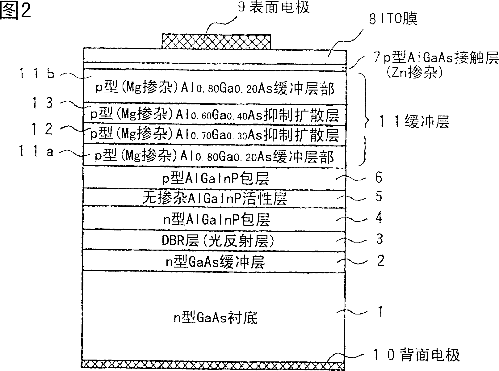
[0099] As Example 1, an epitaxial wafer for a red LED having an emission wavelength around 630 nm having the structure shown in FIG. 2 was produced. The epitaxial growth method, the film thickness of the epitaxial layer, the structure of the epitaxial layer, the electrode formation method and the LED element manufacturing method are as follows.
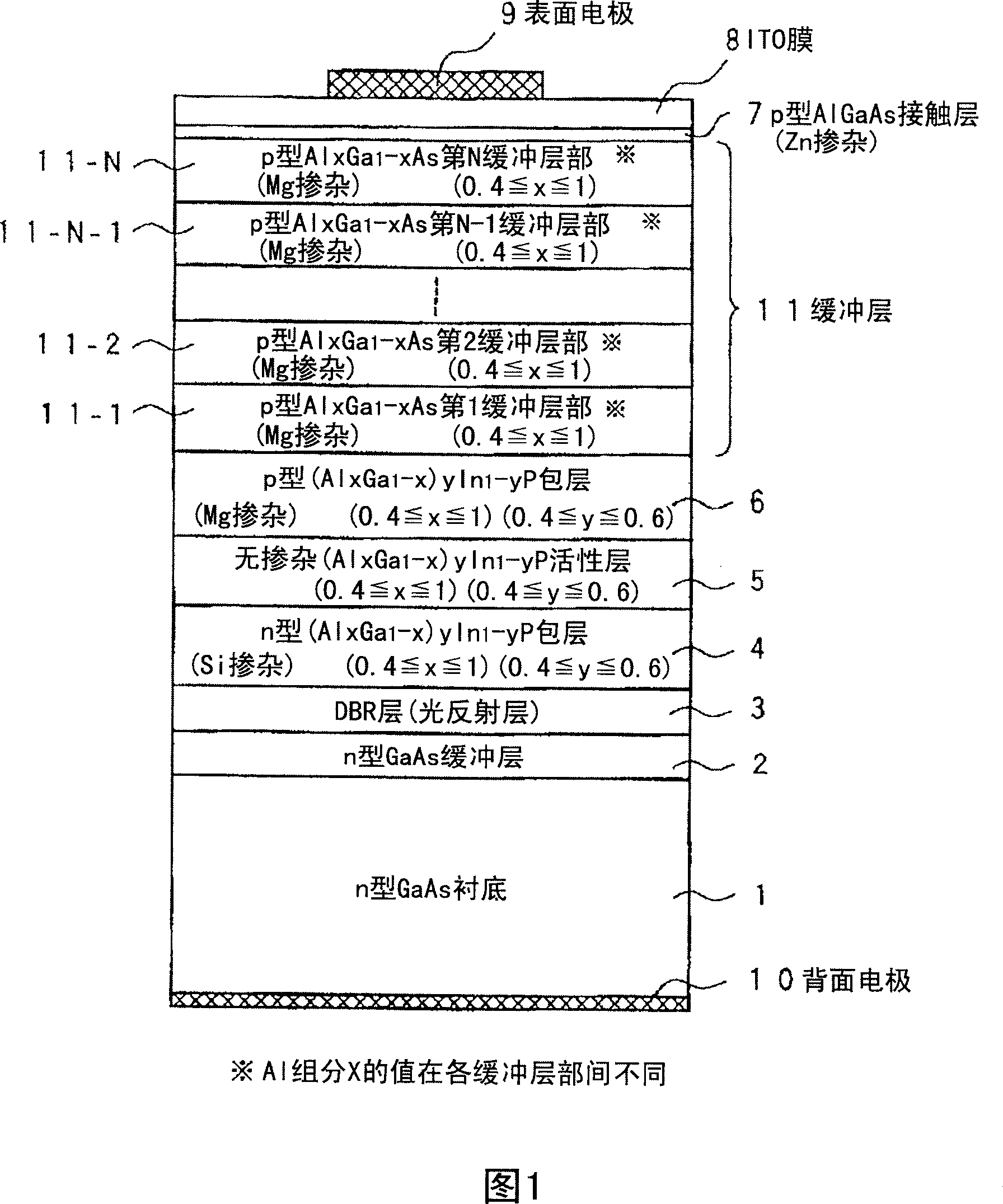
[0100] Using the MOVPE method, the following layers are sequentially stacked and grown on the n-type GaAs substrate 1: n-type (Si-doped) GaAs buffer layer 2 (film thickness 200nm, carrier concentration 1×10 18 / cm 3 ), n-type light reflection layer (so-called DBR layer) 3 (carrier concentration 1×10 18 / cm 3 ), n-type (Si-doped) (Al 0.7 Ga 0.3 ) 0.5 In 0.5 P cladding layer 4 (film thickness 400nm, carrier concentration 7×10 17 / cm 3 ), undoped (Al 0.1 Ga 0.9 ) 0.5 In 0.5 P active layer 5 (film thickness 600nm), p-type (Mg-doped) (Al 0.7 Ga 0.3 ) 0.5 In 0.5 P cladding layer 6 (film thickness 300nm, carrier concentration...
Embodiment 2
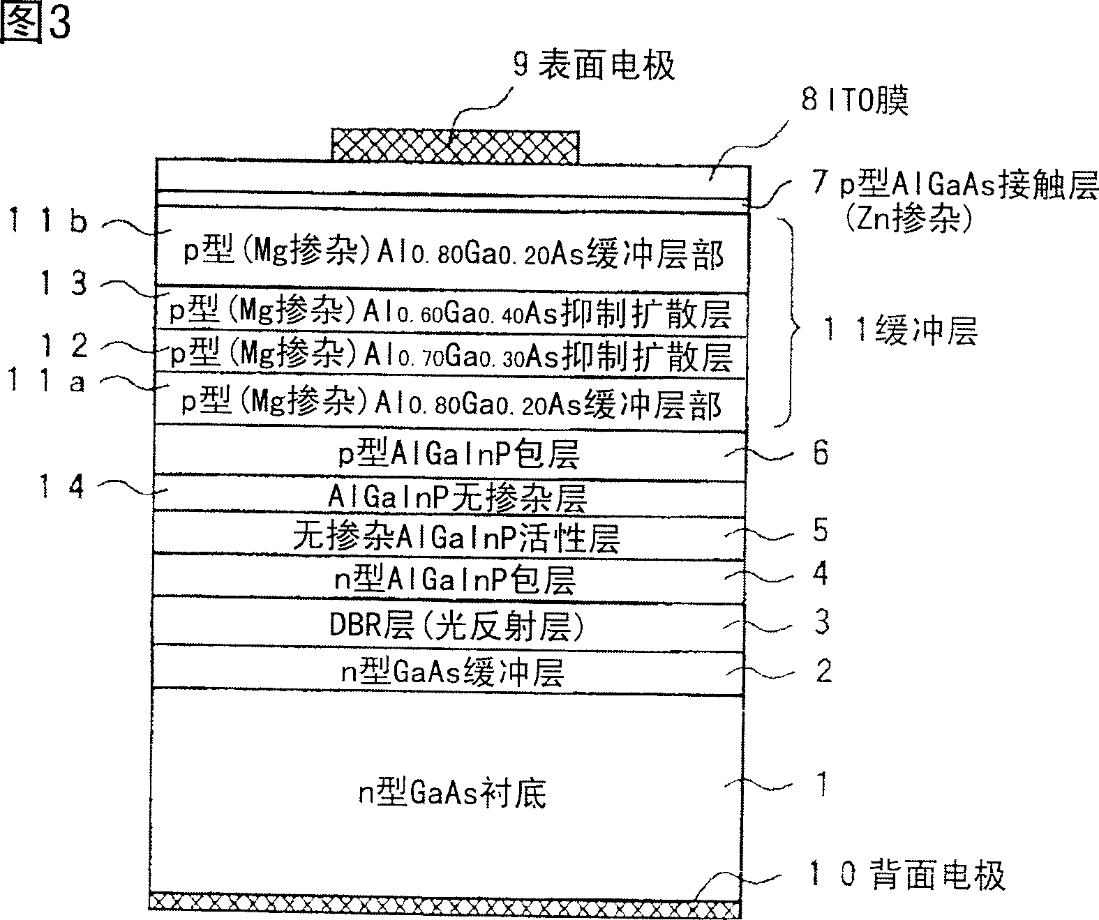
[0116] As Example 2, an epitaxial wafer for a red LED having a light emission wavelength near 630 nm with the structure shown in FIG. 3 was prepared. The epitaxial growth method, the film thickness of the epitaxial layer, the structure of the epitaxial layer and the manufacturing method of the LED element are basically the same as those of the above-mentioned embodiment 1 (FIG. 2). It is different from the above-mentioned Example 1 in the following points.
[0117]In Example 2, a structure is formed in which an undoped layer is provided as the diffusion preventing layer 14 between the above-mentioned active layer 5 and the above-mentioned p-type cladding layer 6 . The diffusion preventing layer 14 is a layer for preventing the p-type dopant diffused from the p-type semiconductor layer above the layer including the p-type cladding layer from being mixed into the active layer 5 . The composition of this diffusion preventing layer 14 is the same as that of the p-type cladding la...
PUM
 Abstract
Description
Claims
Application Information