Supercharge Your Innovation With Domain-Expert AI Agents!

Method of fabricating substrate with nano pattern, light emitting device and manufacturing method thereof

A technology of nanostructures and light-emitting devices, applied in semiconductor devices, electrical components, circuits, etc., can solve problems such as poor mass production capacity, high system cost, and low output

Active Publication Date: 2007-06-20
LG ELECTRONICS INC +1
View PDF0 Cites 6 Cited by
  • Summary
  • Abstract
  • Description
  • Claims
  • Application Information

AI Technical Summary

Problems solved by technology

[0017] To achieve nanometer-precision patterns, precise photolithography techniques such as electron beam lithography, laser holography, and deep ultraviolet steppers are commonly used, but suffer from low yield, high system cost, and poor mass-manufacturability

Method used


Image

  • Method of fabricating substrate with nano pattern, light emitting device and manufacturing method thereof
  • Method of fabricating substrate with nano pattern, light emitting device and manufacturing method thereof
  • Method of fabricating substrate with nano pattern, light emitting device and manufacturing method thereof

Examples


Embodiment Construction

[0030] Preferred embodiments will be described in detail below with reference to the accompanying drawings.

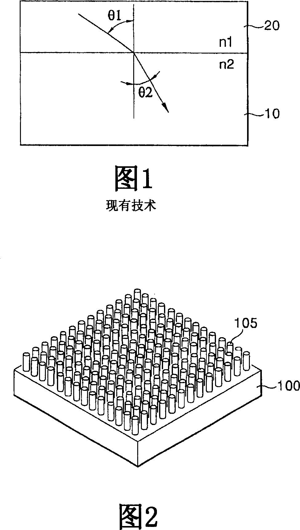
[0031] 2 is a schematic perspective view of an exemplary embodiment of a nanostructured substrate fabricated in accordance with the present invention, wherein the substrate (100) has a plurality of nanorods (105) formed on its top surface, and the plurality of The nanorods (105) include nanostructures.

[0032] The size of each nanorod (105) is 10 nm to 2000 nm, and although the nanorods are shown to be regular in FIG. 2, the nanorods may be arranged irregularly.

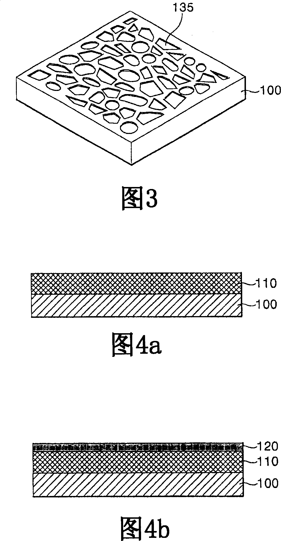
[0033] 3 is a schematic perspective view of another exemplary embodiment of a substrate formed with nanostructures manufactured according to the present invention, wherein the substrate (100) has a plurality of grooves (135) formed on its top surface, and the plurality of Each groove (135) is also nanostructured.

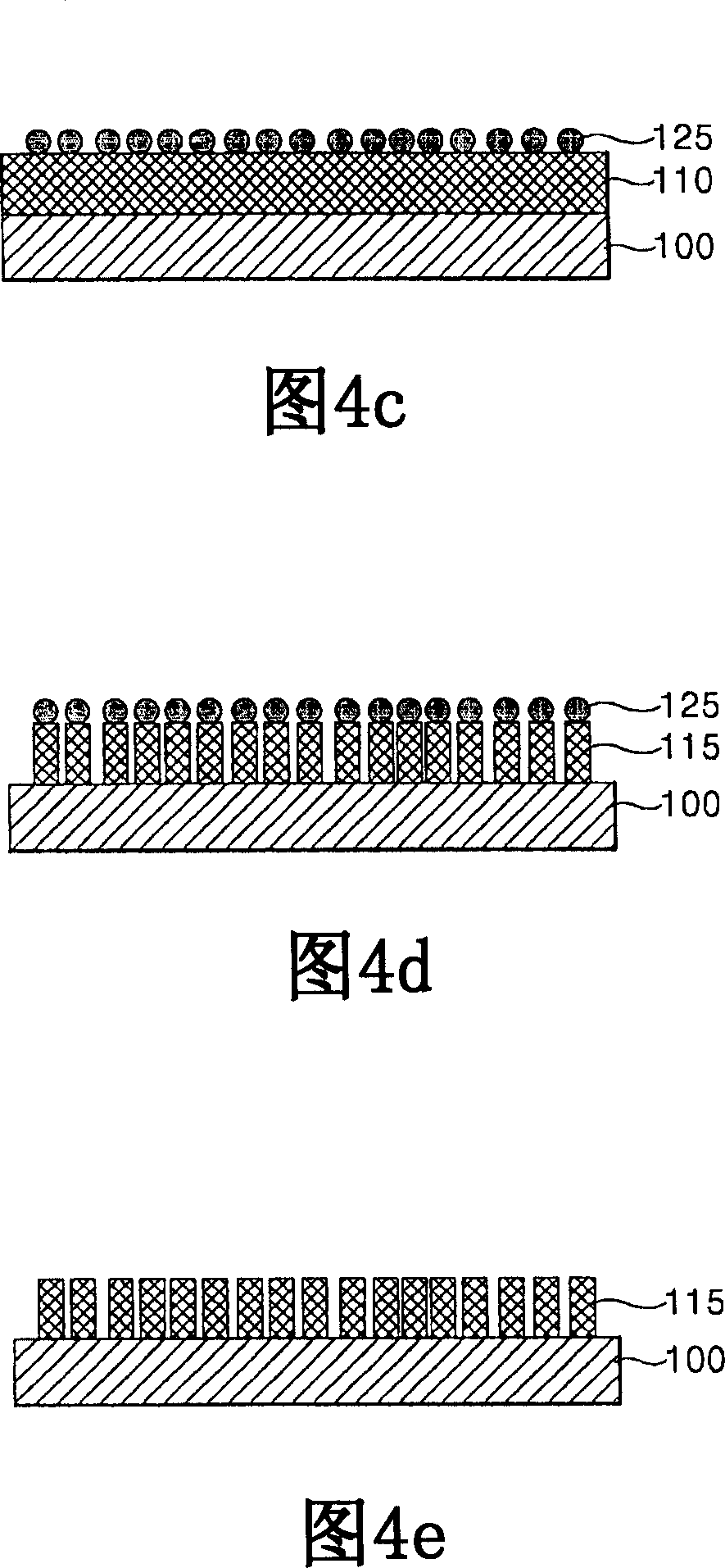
[0034] 4a-4g are cross-sectional views illustrating a method for manufacturing a substrate h...


PUM


Abstract

A method of fabricating a substrate with nano structures, light emitting device using the substrate and a manufacturing method thereof, wherein a substrate for growing a light emitting device is formed with nano agglomerations, and the substrate is etched by using the agglomerations as a mask to allow nano structures to be formed on the substrate, thereby enabling to grow a crystal defect-reduced, reliability-improved, good quality light emitting structure, and wherein the light emitting structure is formed with nano structures to enhance the light extraction efficiency.

Description

[0001] This application claims priority from Korean Patent Application No. 10-2005-0123861 filed with the Korean Intellectual Property Office on December 15, 2005, the disclosure of which is incorporated herein by reference. technical field [0002] The present invention relates to a method for manufacturing a substrate with a nanostructure, a light emitting device and a manufacturing method thereof. Background technique [0003] Common light emitting diodes (LEDs) are single-wave light sources used in a variety of products such as, but not limited to, backlights, signal lights, general lighting applications, and full-color displays. Gallium Nitride (GaN) and ZnO based materials with wide direct-transition bandgap are undergoing extensive research and development and have recently been commercialized in ultraviolet (UV), blue and green wavelengths range of light sources. [0004] Meanwhile, light generated inside the LED is emitted outside the LED, but unfortunately, some o...

Claims


Application Information

Patent Timeline
IPC IPC(8): H01L33/00H01L33/32
CPCH01L33/22H01L33/0079H01L33/007H01L33/0093
Inventor 金钟旭曹贤敬
Owner LG ELECTRONICS INC
Features
  • R&D
  • Intellectual Property
  • Life Sciences
  • Materials
  • Tech Scout
  • Unparalleled Data Quality
  • Higher Quality Content
  • 60% Fewer Hallucinations
Learn More