Dynamic photon crystal producing method

A technology of photonic crystals and production methods, applied in crystal growth, single crystal growth, chemical instruments and methods, etc., can solve the problems of reducing the difficulty of experiments and making them difficult, and achieve the effect of reducing the difficulty of experiments and making experiments flexible and easy

Inactive Publication Date: 2007-06-27
INST OF OPTICS & ELECTRONICS - CHINESE ACAD OF SCI
View PDF0 Cites 6 Cited by
  • Summary
  • Abstract
  • Description
  • Claims
  • Application Information

AI Technical Summary

Problems solved by technology

[0006] The technology of the present invention solves the problem: overcomes the difficult problem of experimental production in the prior art, and provides a method for producing a dynamic photonic crystal, which uses ultrasonic modulation of an acousto-optic crystal to produce a dynamic photonic crystal that does not involve the production of a photonic crystal structure, and has many This kind of acousto-optic crystal can be applied to the present invention. At the same time, the photonic bandgap can be changed by modulating the output electric power and operating frequency of the high-frequency drive power supply, which greatly reduces the difficulty of the experiment and is flexible and easy.

Method used


Image

  • Dynamic photon crystal producing method
  • Dynamic photon crystal producing method

Examples


Embodiment 1

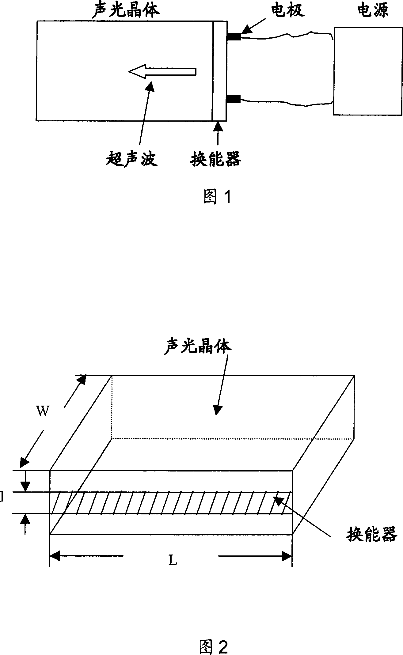
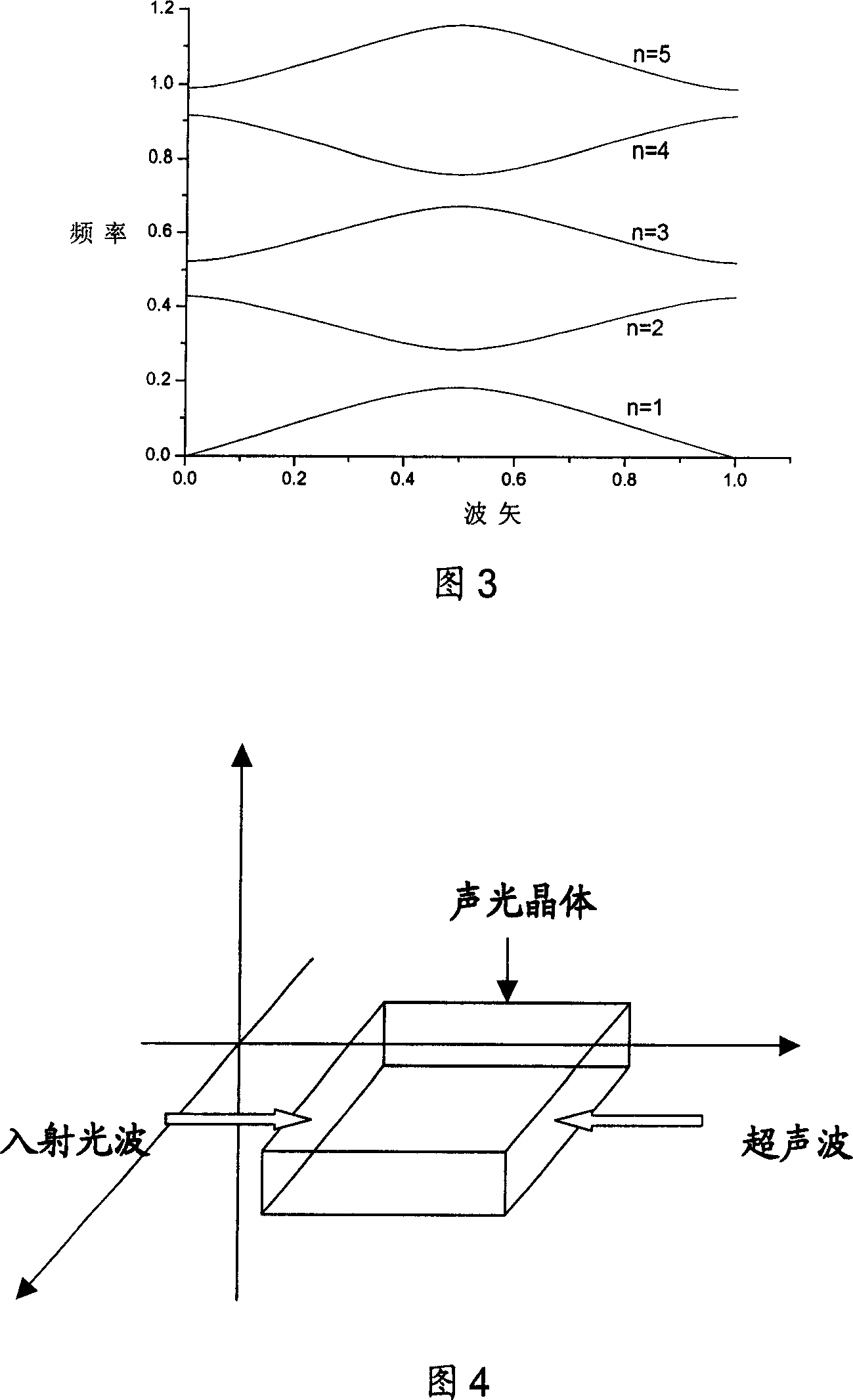
[0029] Embodiment 1 is to use the present invention to make tellurium oxide photonic crystals. Selected tellurium oxide crystal refractive index n 0 =2.26, sound and light merit value M 2 =1200×10 -15 the s 3 / kg, the photonic bandgap of the acousto-optic crystal is proportional to the acousto-optic figure of merit of the acousto-optic crystal, so the crystal with a large acousto-optic figure of merit is selected in the experiment to facilitate the increase of the width of the photonic bandgap. First, the tellurium oxide crystal is polished and oriented, and bonded with the polished piezoelectric transducer, and then the bonded piezoelectric transducer is thinned by mechanical grinding. Plating electrodes on the piezoelectric transducer, the area of ​​the electrodes is 0.25mm 2 , the photonic bandgap of the acousto-optic crystal is inversely proportional to the area of ​​the piezoelectric transducer. In the experiment, the area of ​​the piezoelectric transducer was minimiz...

Embodiment 2

[0030] Embodiment 2 utilizes the present invention to make lead molybdate photonic crystal. Selected lead molybdate crystal refractive index n 0 =2.26, sound and light merit value M 2 =36.3×10 -15 the s3 / kg, the photonic bandgap of the acousto-optic crystal is proportional to the acousto-optic figure of merit of the acousto-optic crystal, so the crystal with a large acousto-optic figure of merit is selected in the experiment to facilitate the increase of the width of the photonic bandgap. First, the lead molybdate crystal is polished and oriented, and bonded with the polished piezoelectric transducer, and then the bonded piezoelectric transducer is thinned by mechanical grinding. Plating electrodes on the piezoelectric transducer, the area of ​​the electrodes is 0.5mm 2 , the photonic bandgap of the acousto-optic crystal is inversely proportional to the area of ​​the piezoelectric transducer. In the experiment, the area of ​​the piezoelectric transducer was minimized to in...

Embodiment 3

[0032] Embodiment 3 is the modulation of ultrasonic waves on tellurium oxide crystals. Selected tellurium oxide crystal refractive index n 0 =2.26, sound and light merit value M 2 =1200×10 -15 the s 3 / kg. First, the tellurium oxide crystal is polished and oriented, and bonded with the polished piezoelectric transducer, then the bonded piezoelectric transducer is thinned by mechanical grinding, and the electrodes are plated on the piezoelectric transducer On the top, the piezoelectric transducer is connected to the high-frequency driving power supply through the electrodes. When the incident light wavelength λ 0 =0.633μm, the selected incident light wavelength should be in the visible light range as far as possible, so as to facilitate the experimental operation. Adjust the electric power and frequency of the high-frequency drive power supply, when the sound and light merit value M 2 =1200×10 -15 the s 3 / kg, the ultrasonic velocity in the tellurium oxide crystal is V...


PUM

PropertyMeasurementUnit
refractive indexaaaaaaaaaa

Abstract

The drive power supply in high frequency combined with piezoelectric transducer generates ultrasonic coupled to acousto-optic crystal. When ultrasonic passes through the acousto-optic crystal, refractive index of material is modulated by strain presents cyclic variation. Acousto-optic crystal possesses photon band gap. Following modulation, photon band gap is changed so as to become dynamic photon crystal.

Description

technical field [0001] The invention relates to a method for generating a dynamic photonic crystal, which belongs to the technical field of photonic crystals. Background technique [0002] Photonic crystal is a kind of artificial material with periodic modulation dielectric function and photonic energy band and bandgap structure. proposed independently. A photonic crystal is a periodic structure composed of materials with different dielectric constants arranged alternately. When electromagnetic waves propagate in it, the light wave dispersion curve forms a band structure, and a "photonic band gap" similar to a semiconductor band gap appears between the bands. The electromagnetic wave whose frequency falls in the forbidden band is strictly prohibited from propagating, so the movement of light in the photonic crystal is controlled by the optical bandgap structure, so the photonic crystal is also called "semiconductor of light". Since the concept of photonic crystals was put ...

Claims


Application Information

Patent Timeline
Patent Type & Authority Applications(China)
IPC IPC(8): G02F1/11G02F1/01C30B5/00
Inventor 张晓玉高洪涛孙祖红钟德蓉严佩英姚汉民
Owner INST OF OPTICS & ELECTRONICS - CHINESE ACAD OF SCI
Why Eureka
Try Eureka