
Light emitting diode and fabrication method thereof

a technology of light-emitting diodes and fabrication methods, which is applied in the manufacture of semiconductor/solid-state devices, semiconductor devices, electrical devices, etc., can solve the problems of low internal quantum efficiency, serious electric leakage of devices, and difficulty in high activation levels, so as to reduce the surface density of v-type defects, increase the mg/ga mole ratio, and reduce the growth rate

Active Publication Date: 2018-10-30
XIAMEN SANAN OPTOELECTRONICS CO LTD
View PDF2 Cites 1 Cited by
  • Summary
  • Abstract
  • Description
  • Claims
  • Application Information

AI Technical Summary

Benefits of technology

The present patent provides a method for improving the efficiency of light emitting diodes (LEDs) by enhancing both internal and external quantum efficiency. The method involves growing a Mg-doped GaN material layer with a high Mg impurity concentration and a thickness of less than or equal to about 250 Å. The P-type layer is formed by a process of electronic blocking layer over the active layer, followed by a thin layer of P-type material. The P-type layer has a low surface density of V-type defects, resulting in improved internal quantum efficiency. The LEDs produced using this method have a high Mg impurity concentration and a reduced surface density of V-type defects, leading to better anti-static electricity capacity and improved external quantum efficiency.

Problems solved by technology

At present, an important factor restricting the improvement of internal quantum efficiency is the hole concentration of the P layer injection in the active region.
As the hole concentration of the P layer is influenced by the doping efficiency and ionization efficiency of Mg in the GaN, it is difficult to achieve high activation level of Mg doping concentration and hole concentration of the P layer, resulting in less holes injected in the active region.
In addition, holes are distributed unevenly, and mainly concentrated in the last 3-5 quantum wells, causing low internal quantum efficiency.
However, in current technologies, if external quantum efficiency is improved solely by thinning the P layer, the V-type defect density of the epitaxial layer surface is bound to be large, causing serious electric leakage of device and poor anti-static electricity capacity.

Method used


Image

  • Light emitting diode and fabrication method thereof
  • Light emitting diode and fabrication method thereof
  • Light emitting diode and fabrication method thereof

Examples


first embodiment

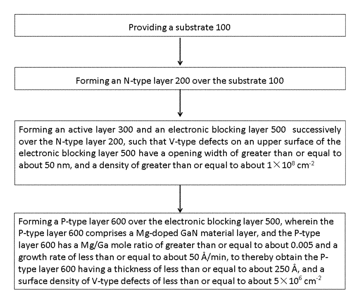
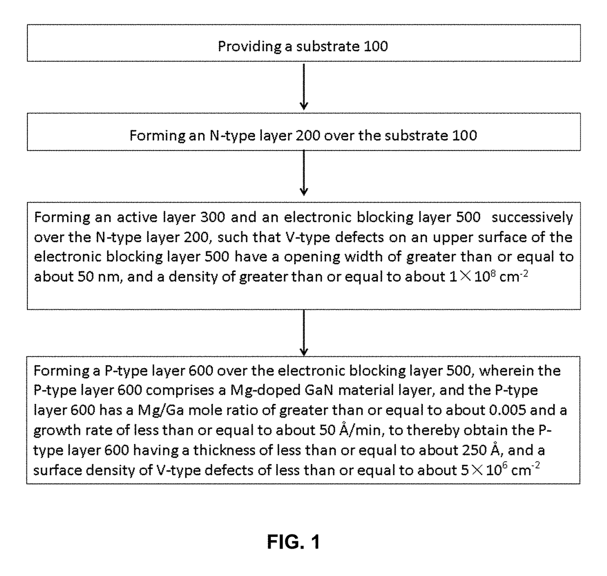
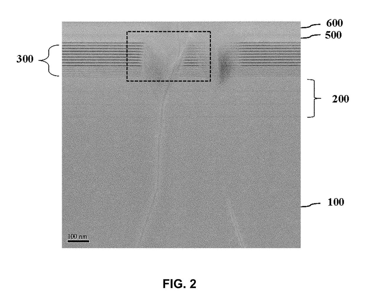
[0056]When the thickness of the P-type layer 600 is less than or equal to about 250 Å,the surface density of V-type defects decreases as the Mg / Ga mole ratio increases, and decreases as the growth rate decreases. Therefore, in this first embodiment of the fabrication method disclosed herein, through a low-rate growth of a highly Mg-doped P-type layer 600, a ratio between a horizontal growth rate and a vertical growth rate during an epitaxial growth can be increased so that the horizontal growth is prominent in epitaxy. As such, the V-type defects can be filled in even when the thickness of the P-type layer 600 is small.

[0057]Meanwhile, the Mg / Ga mole ratio is controlled to be greater than or equal to about 0.005. Because when the Mg / Ga mole ratio is relatively high, it is prone to form MgN through lateral growth, thus an extension of the V-type defects can be inhibited, resulting in an accelerated filling of the V-type defects. As such, a P-type layer 600 having a density of V-type ...

second embodiment

[0065]The above steps in the fabrication method as described above can further improve the performance of the light emitting diode fabricated thereby.

[0066]Herein in the light emitting diode as illustrated in FIG. 7, the electronic blocking layer 500 substantially comprises a non-intentional doping AlGaN layer 510, a P-type AlGaN layer 520, and a P-AlGaN / GaN superlattice structure layer 530, successively over the low-temperature P-type GaN layer 400.

[0067]In the light emitting diode fabricated by the second embodiment of the method, the low-temperature P-type GaN layer 400 is substantially sandwiched between the active layer 300 and the electronic blocking layer 500, which can protect a crystal quality of the active layer 300, in turn facilitating the injection of holes to the active layer 300 to thereby realize a fabrication of a GaN-based light emitting diode with a high light emitting intensity.

[0068]In this second embodiment of the fabrication method, the non-intentional doping ...


PUM


Abstract

A method of fabricating a light emitting diode includes providing a substrate, and forming successively an N-type layer, an active layer, an electronic blocking layer, and a P-type layer over the substrate. The P-type layer includes a Mg-doped GaN material layer having a Mg impurity concentration of about 2×10¹⁹-2×1020 cm−3; and has a thickness of less than or equal to about 250 Å, and has a surface density of V-type defects of less than or equal to about 5×106 cm−2. Through these optimized growth conditions for the P-type layer, the light absorption of the P-type layer can be reduced, the electric leakage due to the relatively large density of V-type defects on the surface can be reduced, and the anti-static capacity of the light emitting diode fabricated thereby can be improved.

Description

CROSS-REFERENCE TO RELATED APPLICATIONS[0001]The present application is a continuation of, and claims priority to, PCT / CN2017 / 087713 filed on Jun. 9, 2017, which claims priority to Chinese Patent Application No. 201610565314.5 filed on Jul. 19, 2016. The disclosures of these applications are hereby incorporated by reference in their entirety.BACKGROUND[0002]GaN-based materials, including InGaN, GaN and AlGaN alloys, are direct gap semiconductors with band gap continuously adjustable from 1.8 to 6.2 eV. Thanks to wide direct gap, strong chemical bond and resistance to high temperature and corrosion, GaN-based materials are ideal for producing light-emitting devices with short wavelengths and high luminance, and are widely applied in fields like full color screen display, LCD backlight source, signal light and lighting.SUMMARY[0003]The inventors of the present disclosure have recognized that the light emitting efficiency of the GaN-based LED can be improved by two ways: one is to impr...

Claims


Application Information

Patent Timeline
Patent Type & Authority Patents(United States)
IPC IPC(8): H01L33/04H01L33/02H01L33/00H01L33/32H01L33/24
CPCH01L33/04H01L33/00H01L33/0075H01L33/32H01L33/025H01L33/24H01L33/02H01L21/0254H01L21/02579H01L21/02458H01L21/02505H01L21/02507H01L21/0262
Inventor CHENG, CHIH-CHINGLING, CHAN-CHANCHANG
Owner XIAMEN SANAN OPTOELECTRONICS CO LTD
Learn More