
Method for preparing graphene, thin-film transistor, array substrate, and display panel

a thin-film transistor and array substrate technology, applied in the field of semiconductor devices, can solve the problems of impurities being introduced, time-consuming and laborious, and the cvd method itself has great defects,

Inactive Publication Date: 2019-03-05
BOE TECH GRP CO LTD
View PDF13 Cites 0 Cited by
  • Summary
  • Abstract
  • Description
  • Claims
  • Application Information

AI Technical Summary

Benefits of technology

[0008]Embodiments of the present invention provide a method for preparing graphene, a thin-film transistor, an array substrate, and a display panel, in which the direct formation of graphene on a target substrate is achieved.
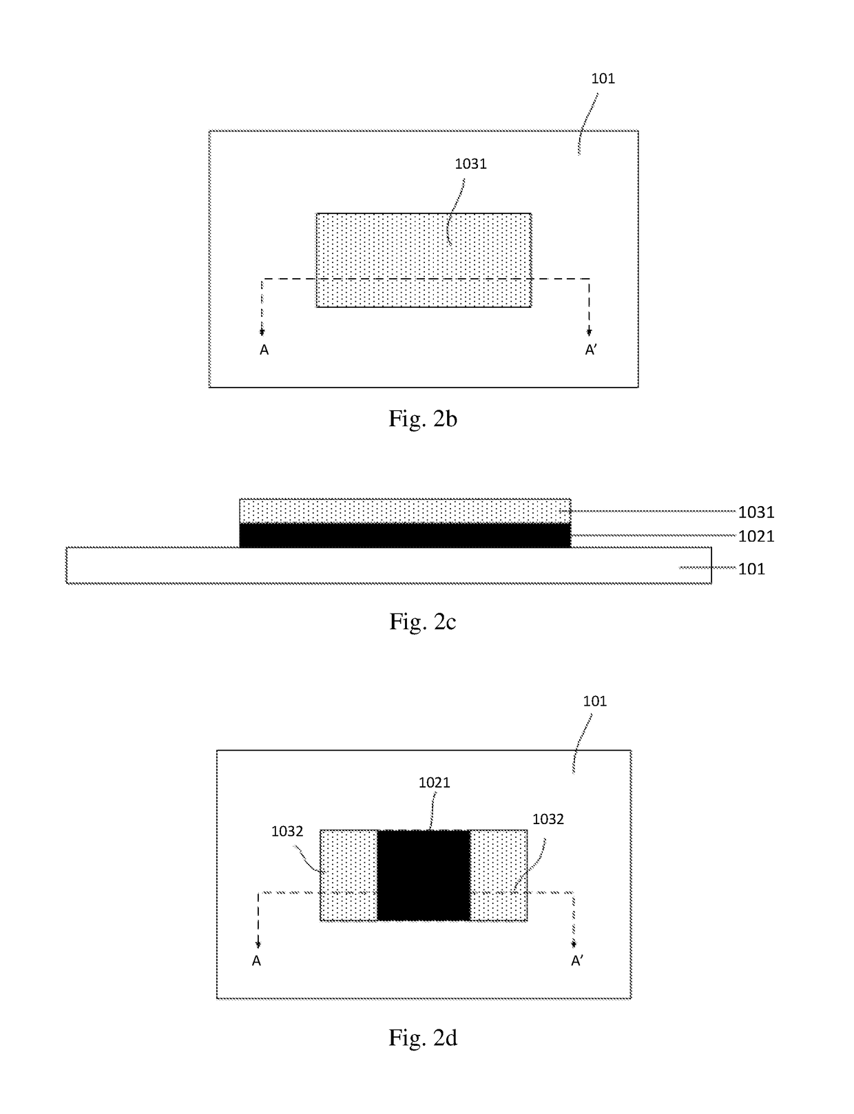
[0013]In the above described method for preparing graphene according to the exemplary embodiment of the present invention, above all, an amorphous carbon thin film and a catalyst metal thin film are formed on a base substrate in this order. Then, the catalyst metal thin film and the amorphous carbon thin film are allowed to form a eutectic at a high temperature caused by an excimer laser in a manner of excimer laser irradiation. When the excimer laser irradiation is finished, the surface temperature of the catalyst metal thin film is drastically decreased, allowing most of carbon atoms of the amorphous carbon thin film to be locked in the catalyst metal thin film and only a small amount of carbon atoms to be precipitated on the lower surface of the catalyst metal thin film, so that a graphene thin film is formed. In the above described method for preparing graphene according to the exemplary embodiment of the present invention, since the graphene thin film is grown by irradiating excimer laser which has minor effect on other film layers located under the graphene thin film, the graphene thin film can be formed directly on the base substrate without a transfer process, compared to the prior art wherein a graphene thin film is prepared in a high-temperature furnace and then the graphene thin film is exfoliated from catalyst metal and transferred to a base substrate. Therefore, damage and contamination of graphene thin films caused by the transfer process can be prevented and properties of prepared graphene thin films are ensured.
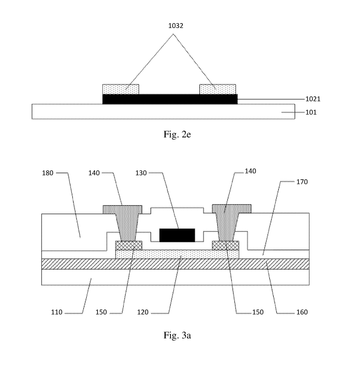
[0027]In the above described thin-film transistor according to the exemplary embodiment of the present invention, the material of the active layer is graphene formed by converting amorphous carbon through excimer laser irradiation under catalysis of the catalyst metal, that is, the active layer of the graphene material is directly formed on a base substrate. Whereas in the prior art, graphene as an active layer is formed by transferring a formed graphene thin film to a base substrate using a transfer process. Therefore, by comparing the above described thin-film transistor to the existing thin-film transistor, problems due to the transfer process of graphene such as damage, contamination, and the like are not prone to occur in the active layer, and thereby properties of the thin-film transistor are improved. Also, as a result of catalyst metal provided on the active layer and at the connection region of the active layer and the source drain electrode, the catalyst metal may protect the active layer from being contaminated by a photoresist in the process of patterning, and thereby properties of the thin-film transistor are further improved. For example, the mobility of a graphene-doped TFT may reach to >1000 cm2 / Vs, and the single-layer graphene of the invention has a light transmittance close to 100% and has good mechanical properties suitable for applications in need of flexibility and the like.
[0028]Preferably, in the above described thin-film transistor according to the exemplary embodiment of the present invention, the catalyst metal is used as the source drain electrode of the thin-film transistor, or the catalyst metal is electrically connected to the active layer and the source drain electrode of the thin-film transistor, in order to simplify the process of preparation.

Problems solved by technology

However, CVD method itself has great defects.
The whole process is time consuming and labor intensive and is not easily controllable.
Furthermore, impurities would be introduced, and even damage of graphene would be caused.
These impurities and defects directly affect electrical properties of graphene.

Method used


Image

  • Method for preparing graphene, thin-film transistor, array substrate, and display panel
  • Method for preparing graphene, thin-film transistor, array substrate, and display panel
  • Method for preparing graphene, thin-film transistor, array substrate, and display panel

Examples


Embodiment Construction

[0040]Embodiments of a method for preparing graphene, a thin-film transistor, an array substrate, and a display panel according to exemplary embodiments of the present invention will be described in details below, in conjunction with accompanying drawings.

[0041]In the accompanying drawings, the size and the shape do not reflect a true proportional relationship in a thin-film transistor and an array substrate, but they are only an illustrative description of the disclosure of the invention.

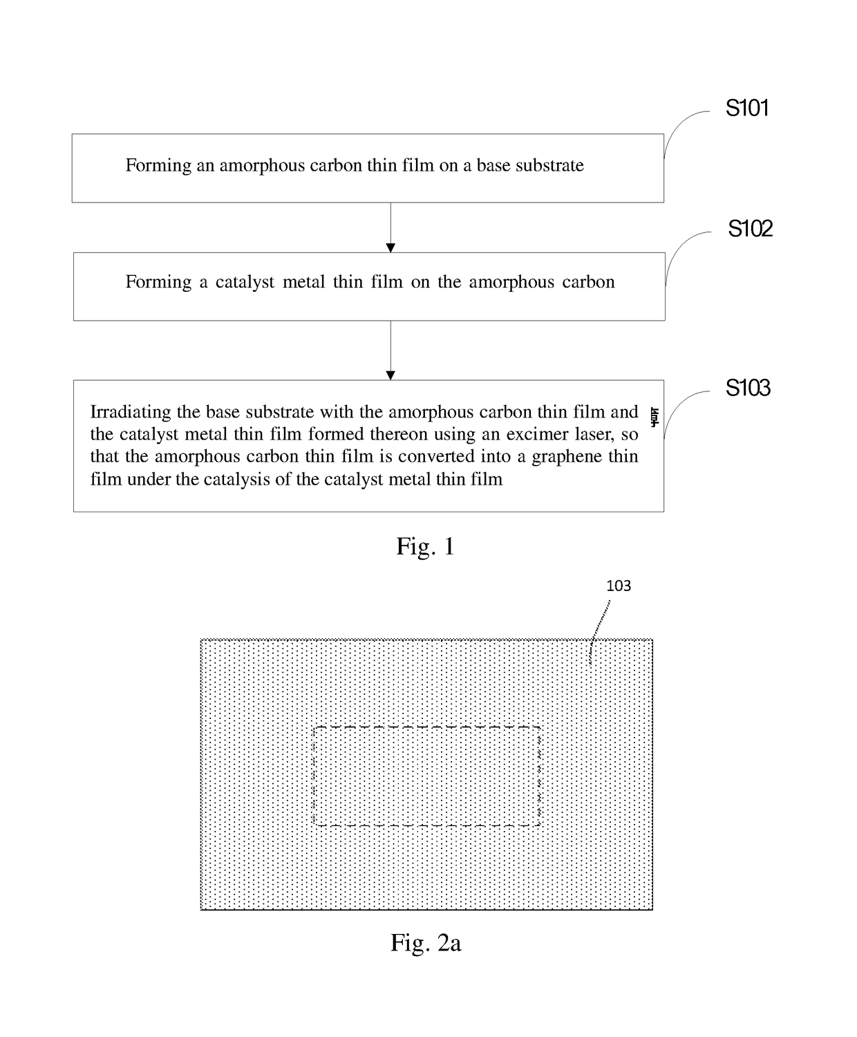
[0042]As shown in FIG. 1, a method for preparing graphene according to an exemplary embodiment of the present invention may comprise the following steps:

[0043]S101, forming an amorphous carbon thin film on a base substrate;

[0044]S102, forming a catalyst metal thin film on the amorphous carbon thin film;

[0045]S103, irradiating the base substrate with the amorphous carbon thin film and the catalyst metal thin film formed thereon using an excimer laser, so that the amorphous carbon thin film is conver...


PUM

PropertyMeasurementUnit
thicknessaaaaaaaaaa
thicknessaaaaaaaaaa
thicknessaaaaaaaaaa

Abstract

This present invention discloses a method for preparing graphene, a thin-film transistor, an array substrate, and a display panel. Above all, an amorphous carbon thin film and a catalyst metal thin film are formed on a base substrate in this order. Then, the catalyst metal thin film and the amorphous carbon thin film are allowed to form a eutectic at a high temperature caused by an excimer laser in a manner of excimer laser irradiation. When the irradiation is finished, the surface temperature of the catalyst metal thin film is drastically decreased, allowing most of carbon atoms of the amorphous carbon thin film to be locked in the catalyst metal thin film and only a small amount of carbon atoms to be precipitated on the lower surface of the catalyst metal thin film, so that a graphene thin film is formed. Since the above described the method employs excimer laser irradiation to grow a graphene thin film, and the excimer laser has minor effect on other film layers located under the graphene thin film, graphene can be formed on the base substrate without a transfer process. Therefore, damage and contamination of graphene thin film caused by the transfer process are prevented and properties of graphene thin film are ensured.

Description

BACKGROUND OF THE INVENTION[0001]Field of the Invention[0002]This invention relates to a technical field of semi-conductors, and specifically to a method for preparing graphene, a thin-film transistor, an array substrate, and a display panel.[0003]Description of the Related Art[0004]Extensive studies on graphene have broken out since single-layer graphene was successfully obtained by a UK physicist, Andre Geim, using a mechanical exfoliation method in 2004. Single-layer graphene is a single-layer hexagonal structure composed of carbon atoms, and has excellent optical, electrical, thermal, and mechanical properties. For example, single-layer graphene has a charge transfer rate of up to about 2×105 cm2 / Vs, which is faster than the charge transfer rate of silicon by 100 times, and has a current density of about 108 A / cm2, which is greater than the current density of copper by 100 times. As a result, single-layer graphene has a significant potential to be used in fields of nanoscale ele...

Claims


Application Information

Patent Timeline
Patent Type & Authority Patents(United States)
IPC IPC(8): H01L21/02H01L29/16H01L29/45H01L29/778H01L29/786H01L21/268C01B32/184H01L29/66
CPCH01L21/268C01B32/184H01L21/02527H01L21/02672H01L21/02686H01L29/78684H01L29/45H01L29/66045H01L29/66742H01L29/778H01L29/78633H01L29/1606
Inventor SUN, TUO
Owner BOE TECH GRP CO LTD
Learn More