
Method for reducing the surface roughness of a thin layer of conductive oxides

Inactive Publication Date: 2007-05-31
CONSIGLIO NAT DELLE RICERCHE
View PDF1 Cites 0 Cited by
  • Summary
  • Abstract
  • Description
  • Claims
  • Application Information

AI Technical Summary

Benefits of technology

[0010] The purpose of the present invention is to provide a method for reducing the surface roughness of a thin layer for thin-layer opto-electronic devices in order to cut down the drawbacks mentioned above and, consequently, increase the durability of thin-layer opto-electronic devices in a simple and economically advantageous manner.
[0011] According to the present invention, there is provided a method for reducing the surface roughness of a thin layer for thin-layer opto-electronic devices according to what is claimed in claim 1.

Problems solved by technology

Even though OLEDs form a subject of considerable interest for the industry, they still present a relatively limited durability.
The relatively poor durability is linked to the appearance of dark spots.
Recently, it has been noted that one of the causes of the poor durability of OLEDs is the surface morphology of the anode.
The relatively high surface roughness of the thin ITO layer and the presence of differences in height between peak and trough comparable to the overall thickness of the intermediate layers, i.e., some tens of nanometres, appear to be one of the causes of the relatively low durability of OLEDs.
The effects produced by the relatively high roughness could be multiple: for example, there could occur a non-uniform and very disorderly growth of the intermediate layers in contact with the ITO layer and / or an increase in the effective electrical field in the areas of the peaks.

Method used


Image

  • Method for reducing the surface roughness of a thin layer of conductive oxides
  • Method for reducing the surface roughness of a thin layer of conductive oxides
  • Method for reducing the surface roughness of a thin layer of conductive oxides

Examples


example 1

[0046] This example describes polishing of a commercially available thin ITO layer.

[0047] A commercially available thin ITO layer, which has a thickness of approximately 100 nm and is supported by a plate of glass, was polished using an abrasive compound and a polishing cloth.

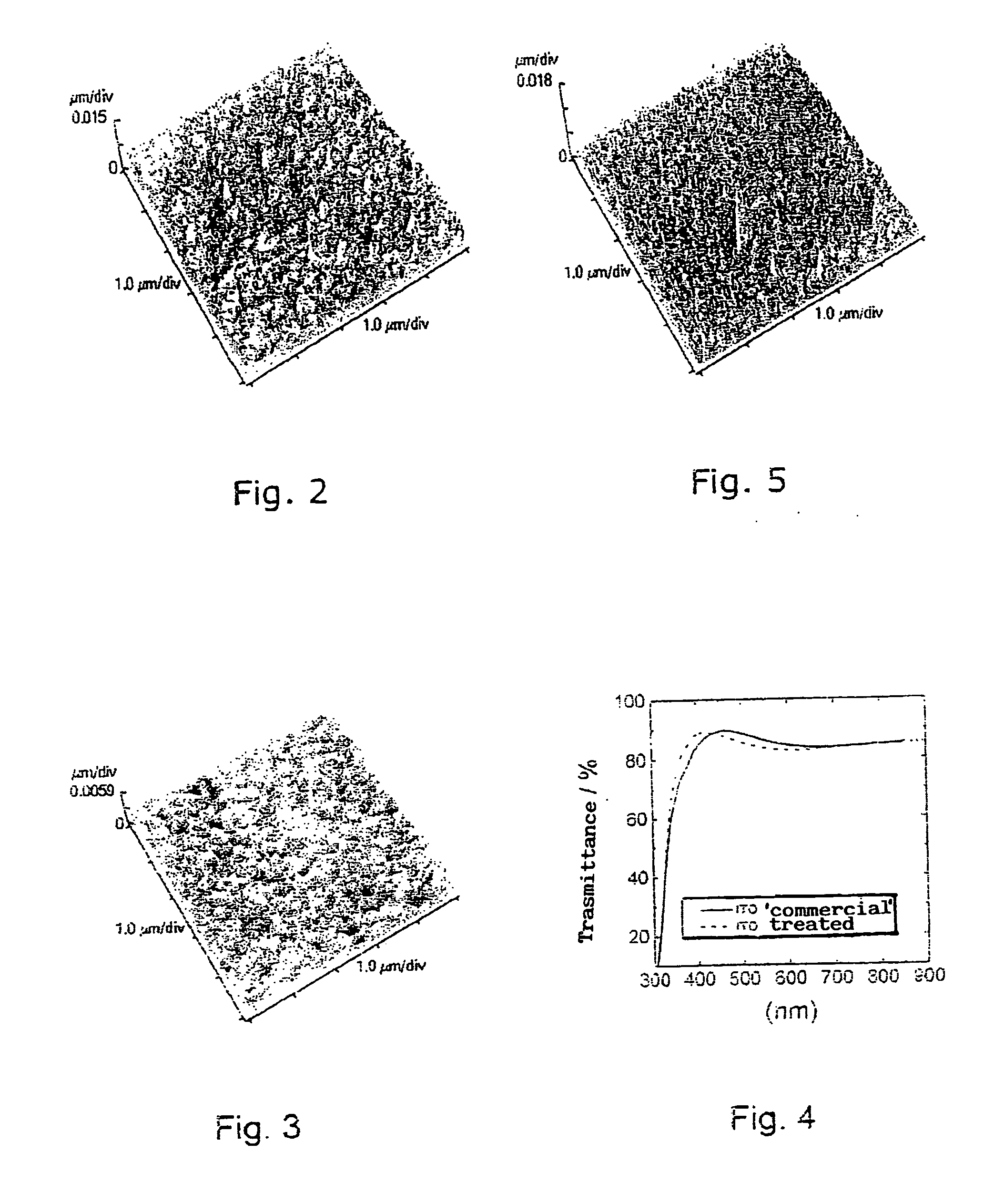
[0048] The commercially available thin ITO layer, the surface morphology of which is illustrated in FIG. 2, was formed by aggregates having planar dimensions of approximately 100-200 nm, with a maximum difference in height between peak and trough of approximately 31 nm and mean roughness of approximately 1.9 nm.

[0049] The polishing cloth was a woven finishing cloth and was made of synthetic fabric. The abrasive compound was obtained by diluting a colloidal solution, which comprised silica particles having a diameter of between 5 nm and 150 nm and dispersed in a basic solution of potassium hydroxide (the colloidal solution used is known by the commercial name Syton HT-50® and is produced by Dupont®), in deion...

example 2

[0052] This example describes polishing of a thin ITO layer prepared in the laboratory.

[0053] A thin ITO layer prepared in the laboratory, which had a thickness of approximately 100 nm and coated a plate of glass, was polished using an abrasive compound and a polishing cloth.

[0054] The thin ITO layer prepared in the laboratory, the surface morphology of which is illustrated in FIG. 5, had aggregates having planar dimensions of between approximately 50 nm and 100 nm, with a maximum difference in height between peak and trough of approximately 54 nm and a mean roughness of approximately 1.9 nm.

[0055] Polishing was carried out according to what is described in Example 1 so as to obtain the treated ITO layer substantially identical to the treated ITO layer described in Example 1.

example 3

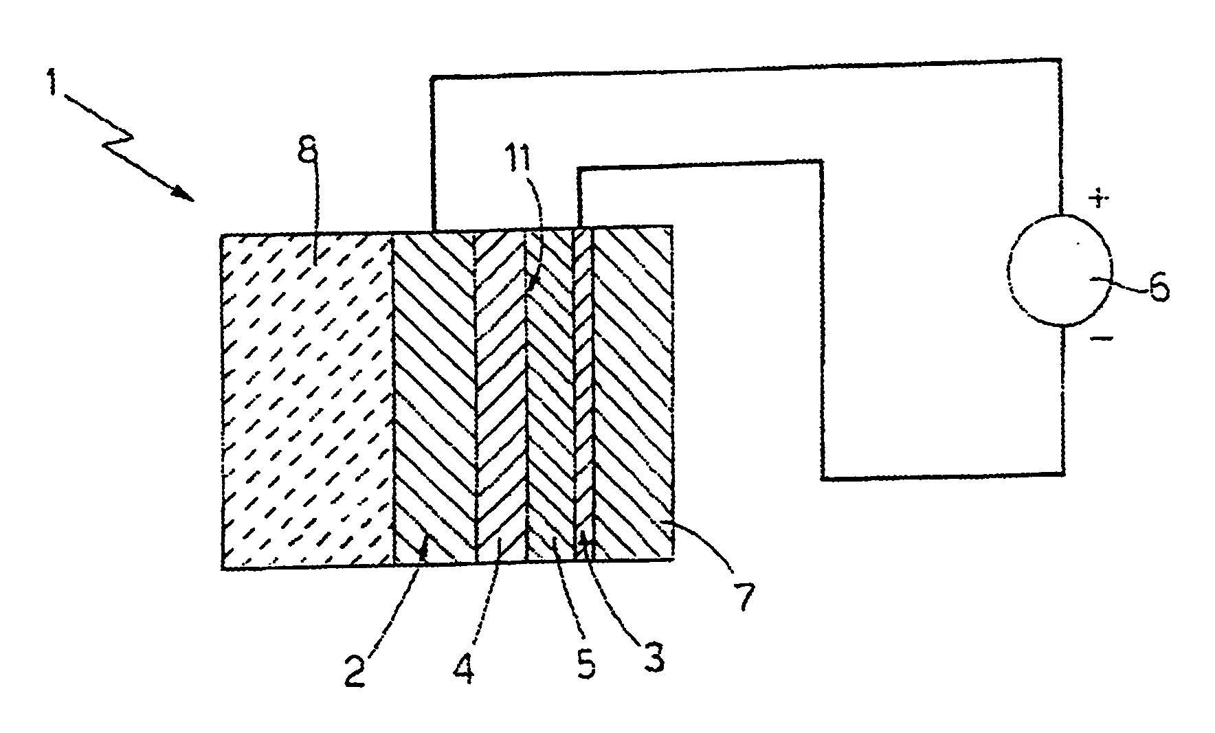
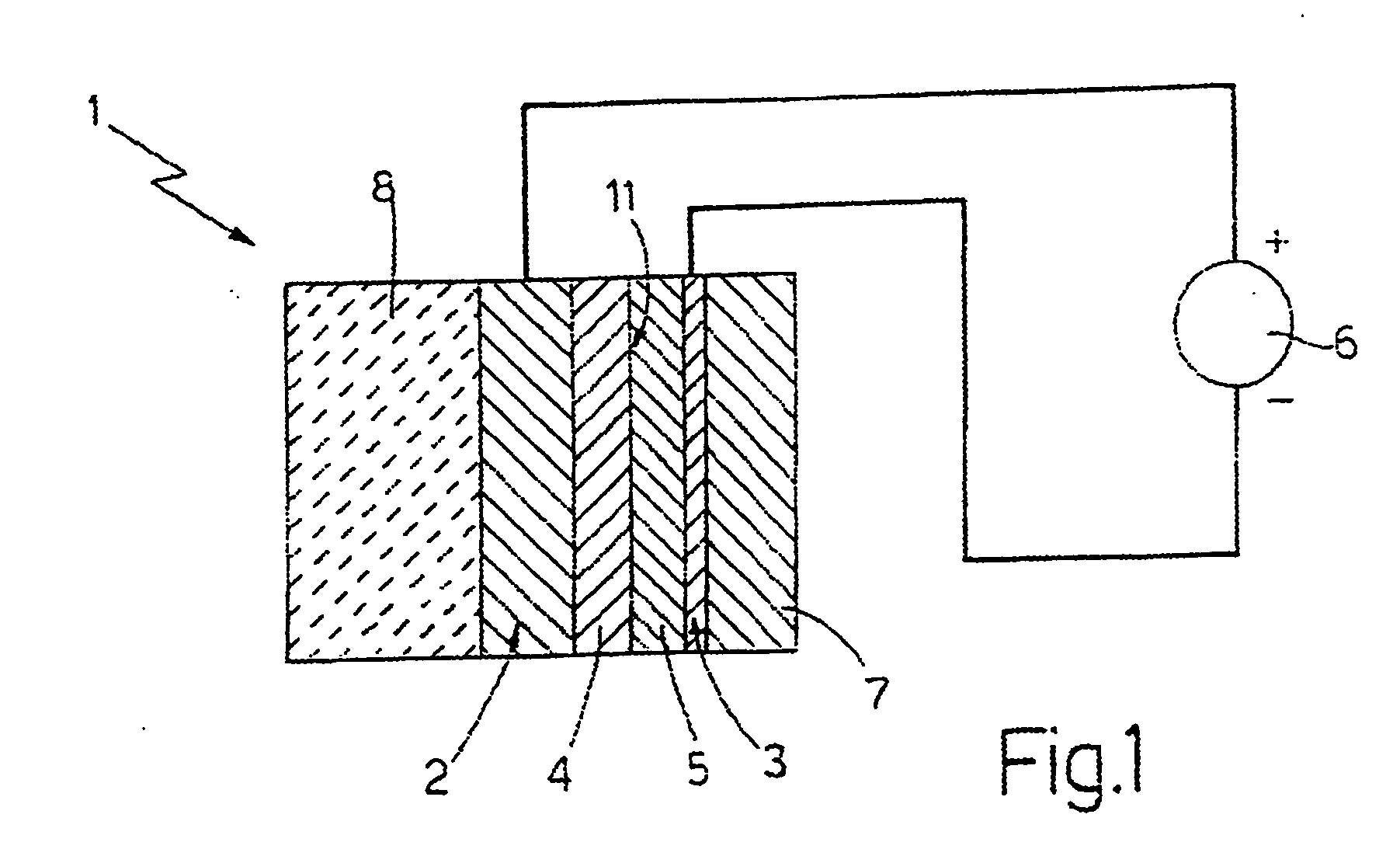
[0056] An organic electroluminescent device was prepared in the manner described in what follows.

[0057] A plate of glass coated with a thin ITO layer, which was treated according to Example 1 or Example 2, was cleaned by being dipped in a boiling solution of acetone and alcohol and by subsequently being laid for approximately thirty minutes in an ultrasound washing machine.

[0058] At this point, the following layers were deposited, in succession, one on top of the other, by sublimation in a high-vacuum evaporator and at a pressure of 8×10⁻⁴ Pa, on the coated plate of glass: a layer of 4,4′,4′″-Tri(N,N-diphenyl-amino)-triphenyl amine (TDATA) having the thickness of 60 nm; a layer of 3-(4-diphenylyl)-4-phenyl-5-ter-butylphenyl-1,2,4-triazole (PBD) having the thickness of 60 nm; a layer of calcium having the thickness of 25 nm; and a layer of silver having the thickness of 100 nm.

[0059] The ITO layer and the calcium layer were connected to an external generator.


PUM


Abstract

A method for reducing the surface roughness of thin layers of conductive oxides for thin-layer opto-electronic devices envisages polishing with a finishing cloth and an abrasive compound, which has a basic pH and contains silica particles.

Description

TECHNICAL FIELD [0001] The present invention relates to a method for reducing the surface roughness of a thin layer for thin-layer opto-electronic devices. [0002] The present invention finds advantageous application in the field of organic electroluminescent devices (OLEDs), to which the ensuing treatment makes explicit reference without, however, this implying any loss of generality. BACKGROUND ART [0003] Organic electroluminescent devices known as organic light emitting diodes (OLEDs) are light emitting devices which comprise one or more intermediate layers set between a cathode and an anode, which is usually constituted by a thin conductive layer made of indium and tin oxide (ITO) supported by a plate of glass. At least one of the intermediate layers comprises organic material. [0004] The intermediate layers and the cathode and anode layers present in OLEDs are usually obtained via known techniques of spin coating and / or dipping, or else evaporation and / or high-vacuum cathodic sp...

Claims


Application Information

Patent Timeline
IPC IPC(8): H01J1/62H01J63/04H01L51/00H01L51/30H01L51/40H01L51/52
CPCH01L51/0001H01L51/005H01L51/0059H01L51/5206H10K71/00H10K85/60H10K85/631H10K50/81
Inventor COCCHI, MASSIMODI MARCO, PIERGIULIOFATTORI, VALERIAGIRO, GABRIELEVIRGILI, DALIAGARULLI, ALBERTO
Owner CONSIGLIO NAT DELLE RICERCHE
Learn More