
Electronically pumped surface-emitting photonic crystal laser

a photonic crystal laser and electric pump technology, applied in the direction of lasers, laser optical resonators, semiconductor lasers, etc., can solve the problems of difficult input of electric current, and achieve the effect of slowing down the loss on the boundary

Active Publication Date: 2019-07-02
PHOSERTEK CORP
View PDF3 Cites 13 Cited by
  • Summary
  • Abstract
  • Description
  • Claims
  • Application Information

AI Technical Summary

Benefits of technology

This patent aims to provide an electrically pumped surface-emitting photonic crystal laser with an epitaxy structure etched towards the inside from the top to fabricate a photonic crystal. This laser has indium tin oxide fabricated as electrodes for the laser to emit lasers and to possess conductivity without the complicated process of wafer fusion bonding and epitaxy regrowth in the conventional manufacturing process. The invention also has a transparent conducting layer made of ITO, which helps to control electric currents and slow down the loss on boundaries of the photonic crystals, resulting in the successful emission of laser beams at room temperature. The technical effects of this patent include simplifying the manufacturing process and improving the efficiency of the laser.

Problems solved by technology

However, input of electric currents is difficult due to the lattice structure of photonic crystals; the routes for light transmission and distribution of the carriers are issues to be considered.

Method used


Image

  • Electronically pumped surface-emitting photonic crystal laser
  • Electronically pumped surface-emitting photonic crystal laser
  • Electronically pumped surface-emitting photonic crystal laser

Examples


Embodiment Construction

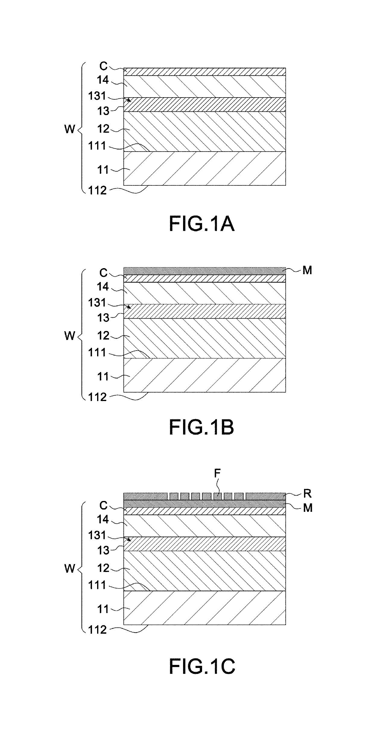
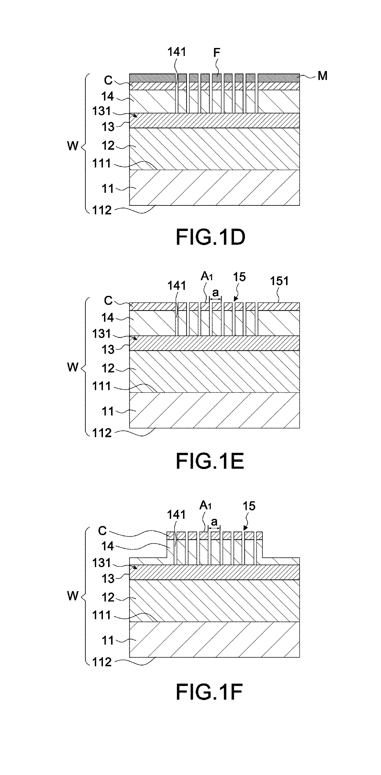
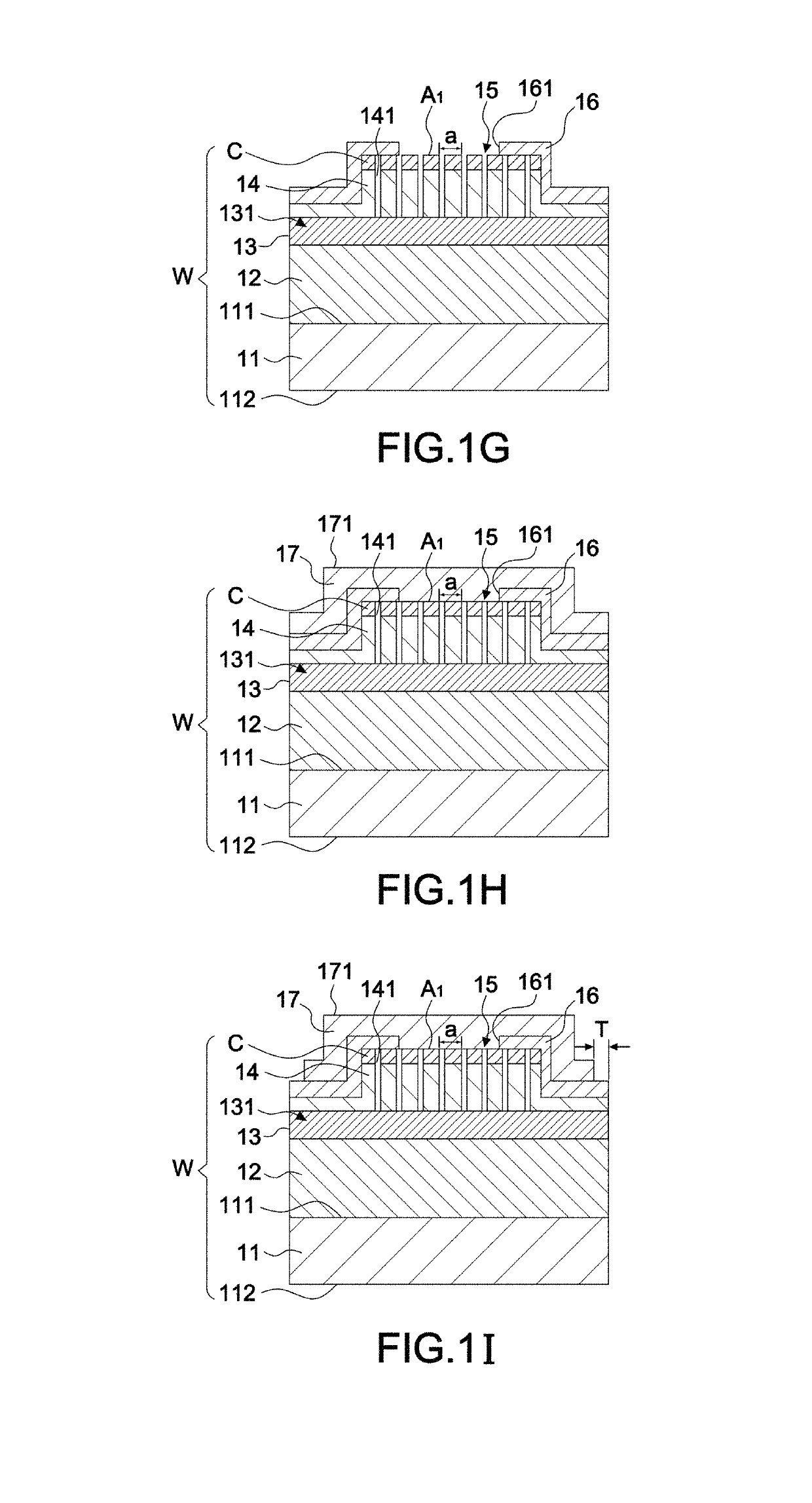
[0042]Referring to FIGS. 1A-1L, in a preferred embodiment, an electrically pumped surface-emitting photonic crystal laser 10A mainly includes a substrate 11, a first cladding layer 12, an active layer 13, a second cladding layer 14, a contact layer C, a hard mask M, a photonic crystal structure 15, an electrical currents confining structure 16, a transparent conducting layer 17, a metal anode 18 and a metal cathode 19.

[0043]The substrate 11 has a top surface 111 and a bottom surface 112. In this embodiment, the substrate 11 is made of a material selected from a group consisting of gallium nitride (GaN), gallium arsenide (GaAs) and indium phosphide (InP), but it is not limited to such composition.

[0044]The first cladding layer 12 is arranged on the top surface 111 of the substrate 11. In this embodiment, the first cladding layer 12 is made of a material selected from a group consisting of aluminum gallium arsenide (AlGaAs), GaAs, aluminum gallium nitride (AlGaN), aluminum gallium ind...


PUM


Abstract

An electrically pumped surface-emitting photonic crystal laser includes an electric currents confinement structure arranged on a photonic crystal structure and an active layer with an opening, a transparent conducting layer arranged on the electric currents confinement structure and covering the photonic crystal structure, a metal anode arranged on the transparent conducting layer with an aperture. The photonic crystal laser has its epitaxy structure etched from above to fabricate the photonic crystal to allow laser beams to pass through with conductivity for the purpose of electrically pumping a quantum structure without complex technologies of wafer fusion bonding or epitaxial regrowth. Thereby the laser beams can be emitted from a front surface of the epitaxy structure with a narrow divergence angle.

Description

BACKGROUND OF THE INVENTION1. Field of the Invention[0001]The invention relates to an electrically pumped surface-emitting photonic crystal laser that has a metal anode, a transparent conducting layer and an electrical currents confining structure combined to electrically pump a quantum structure thereof for a photonic crystal structure thereof to emit lasers from a surface of an epitaxy structure thereof.2. Description of the Related Art[0002]Photonic crystals are periodic metamaterials that can be fabricated by modern technology with features similar to solid crystals. In solid crystals, a band structure can be discovered from its dispersion relation; therefore, the same structure can be seen in photonic crystals as well. Furthermore, photonic crystals have forbidden band where electromagnetic waves with specific frequency cannot exist within as solid crystals have bandgaps. With the similarities, photonic crystals are able to control transmission of lights and therefore have been...

Claims


Application Information

Patent Timeline
IPC IPC(8): H01S5/00H01S5/10H01S5/042H01S5/22H01S5/18H01S5/343H01S5/34H01S5/183H01S5/185
CPCH01S5/0425H01S5/2205H01S5/18H01S5/343H01S5/0421H01S5/18308H01S5/105H01S5/18319H01S5/18344H01S5/18394H01S5/34H01S5/22H01S5/04253H01S5/04252H01S5/3215H01S5/323H01S5/3054H01S5/3412H01S2301/176H01S5/11H01S5/185
Inventor LIN, KUO-JUIHSU, MING-YANGCHEN, YU-CHEN
Owner PHOSERTEK CORP
Learn More