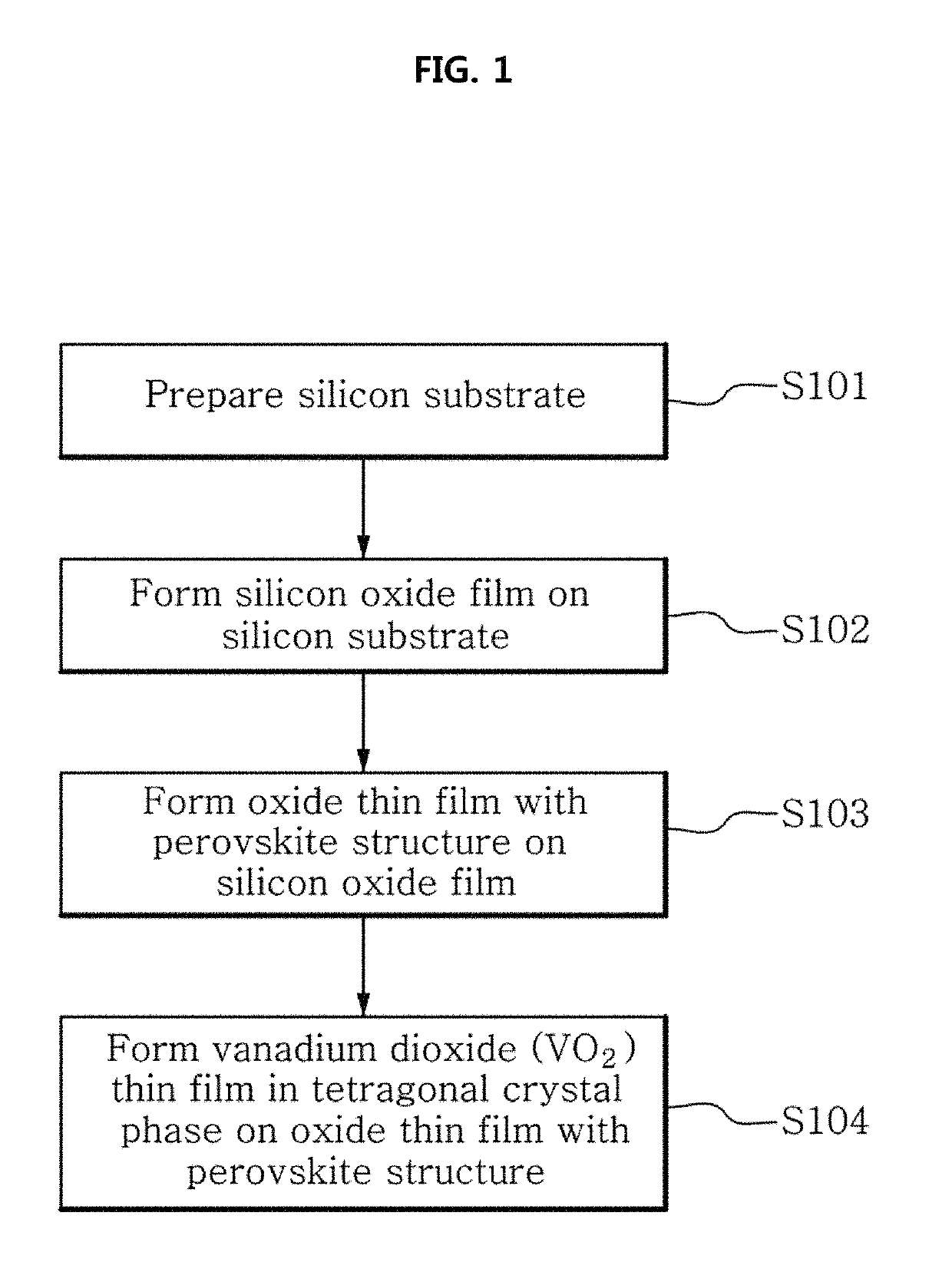
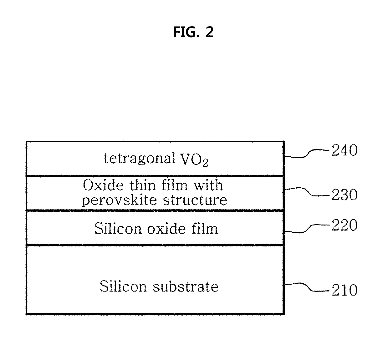
Thin film structure for micro-bolometer and method for fabricating the same
a technology of resistors and bolometers, which is applied in the direction of photometry using electric radiation detectors, optical radiation measurement, instruments, etc., can solve the problems of difficult use of bolometers, difficult to achieve the effect of high tcr, superior properties, and low resistan
- Summary
- Abstract
- Description
- Claims
- Application Information
AI Technical Summary
Benefits of technology
Problems solved by technology
Method used
Image

Examples
experimental example 1
nal VO2 / SrTiO3 Thin Film
[0044]A VO2 thin film in tetragonal crystal phase was formed on a SrTiO3 thin film at the thickness of 54 nm through a sputtering process. A sputtering target was VO2 in monoclinic crystal phase, and the process pressure was set to 5-20 mTorr, the process temperature was set to 200-500° C., and mixed gas of O2 and Ar was supplied into a sputtering chamber at a ratio of O2 / (Ar+O2)=0.2-0.3%.
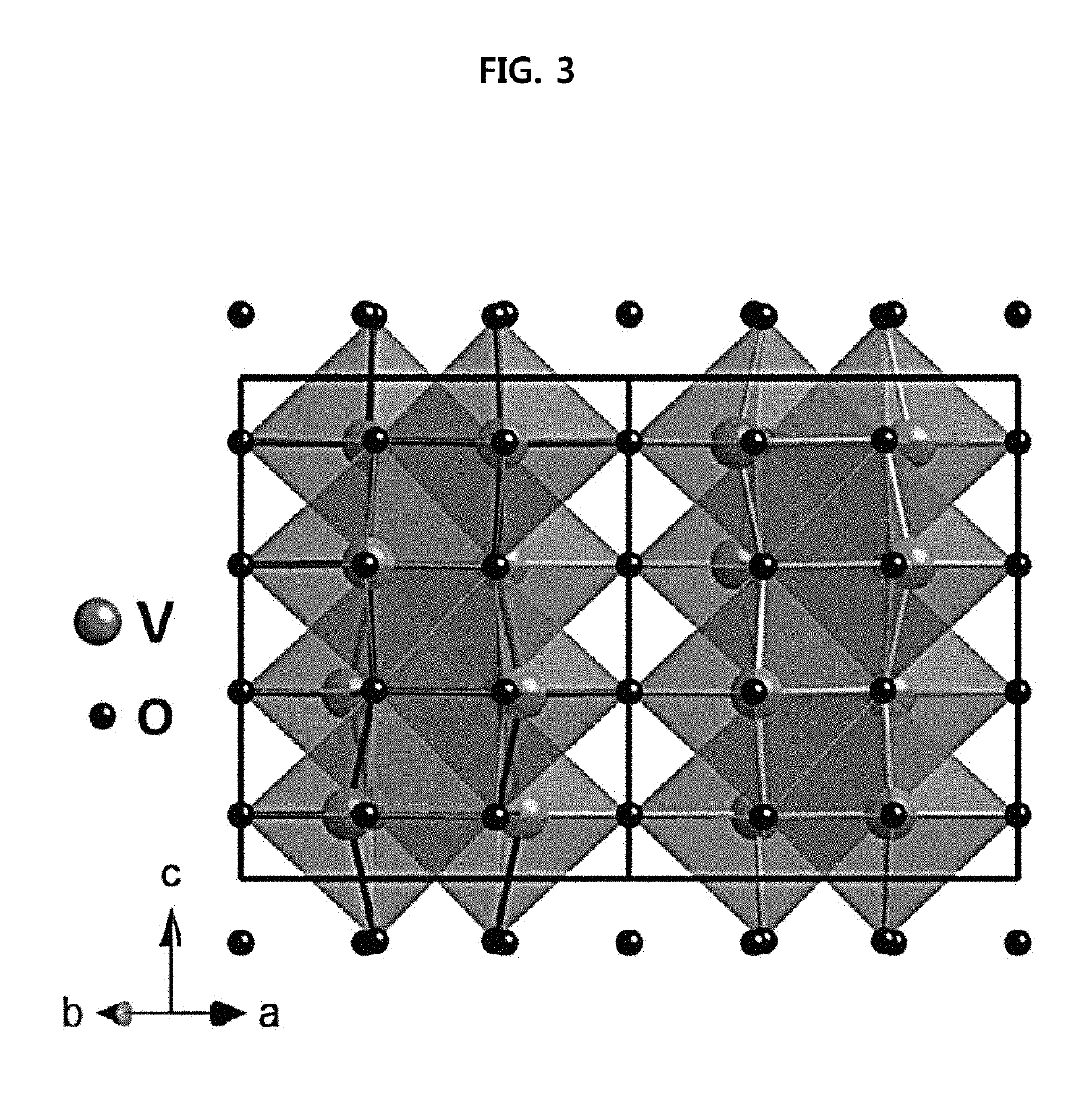
[0045]As a result of conducting X-ray diffraction analysis of the tetragonal VO2 / SrTiO3 thin film fabricated through experimental example 1, it can be seen that peak for tetragonal VO2 crystal phase (′VO2(A)′ in FIG. 4B) appears as shown in of FIG. 4B, and this confirms that VO2 grown on the SrTiO3 thin film is tetragonal VO2 crystal phase. On the contrary, when an oxide thin film with perovskite structure is not used, it can be seen that various crystal phases of vanadium dioxide such as VO2(A), V2O5 and V3O7 exist together as shown in of FIG. 4A.
Experimental Example 2: Cha...
PUM
| Property | Measurement | Unit |
|---|---|---|
| thickness | aaaaa | aaaaa |
| thickness | aaaaa | aaaaa |
| temperature | aaaaa | aaaaa |
Abstract
Description
Claims
Application Information