
Reduction in the annealing temperature of an IGZO layer obtained by sol gel

a technology of sol gel and igzo layer, which is applied in the direction of transistors, semiconductor/solid-state device manufacturing, electrical equipment, etc., can solve the problems of temperature incompatibility with implementation on certain supports, in particular on polymer supports, and the annealing temperature required for its activation is limited, and the effect of non-uniform composition

Inactive Publication Date: 2019-08-13
COMMISSARIAT A LENERGIE ATOMIQUE ET AUX ENERGIES ALTERNATIVES
View PDF5 Cites 2 Cited by
  • Summary
  • Abstract
  • Description
  • Claims
  • Application Information

AI Technical Summary

Benefits of technology

The patent is about a method to make sure a polymer or plastic substrate is properly heated during a process. This method uses a heat treatment along with a pulsed photon treatment to improve the annealing (a process where materials are heated to bring them to the desired temperature) of the substrate. The pulsed photon treatment helps to heat the substrate without causing damage, while the heat treatment improves the process. Overall, this method allows for lower annealing temperatures and makes it possible to use the polymer or plastic substrate in various applications.

Problems solved by technology

Such a method requires the establishment of a high vacuum, may cause composition non-uniformities, and may prove to be costly.
Such temperatures may prove to be incompatible with implementation on certain supports and in particular on polymer supports.
The problem is posed of finding a novel method for producing a layer based on metal oxide of IXZO type in which the annealing temperature required for its activation would be limited.

Method used


Image

  • Reduction in the annealing temperature of an IGZO layer obtained by sol gel
  • Reduction in the annealing temperature of an IGZO layer obtained by sol gel
  • Reduction in the annealing temperature of an IGZO layer obtained by sol gel

Examples


Embodiment Construction

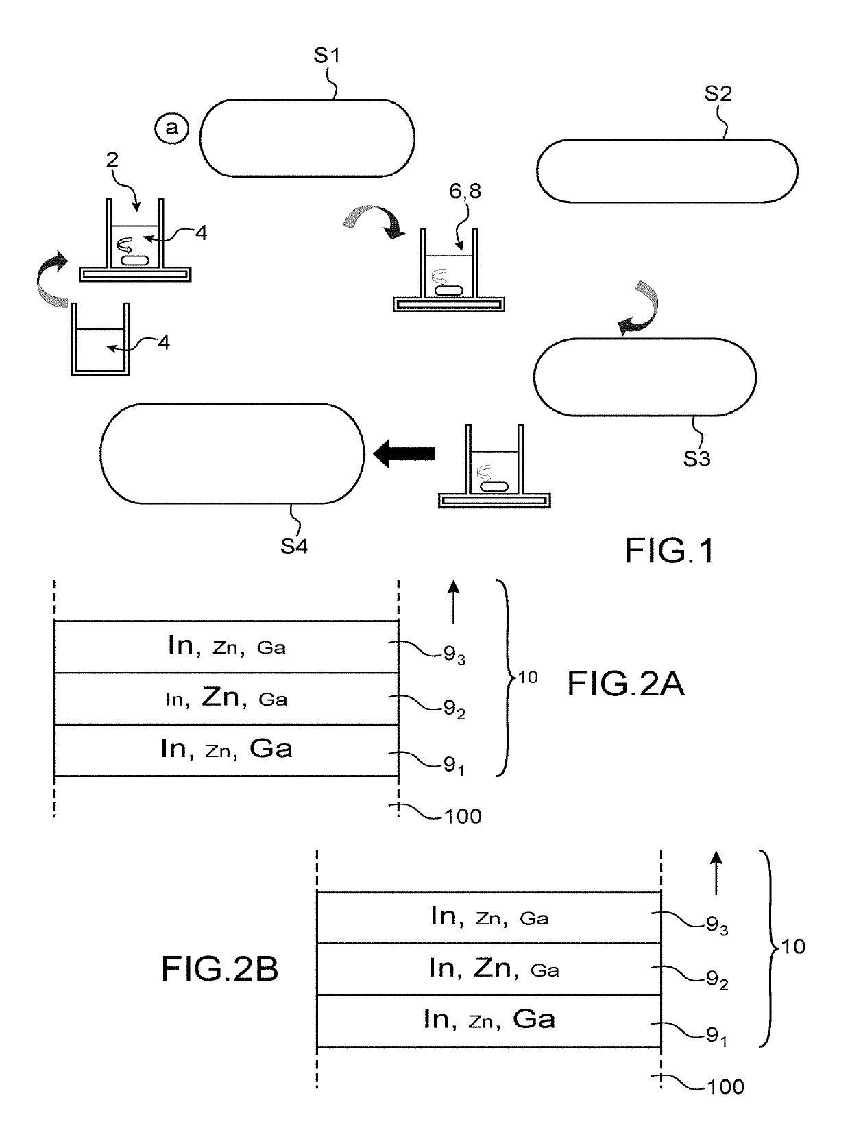
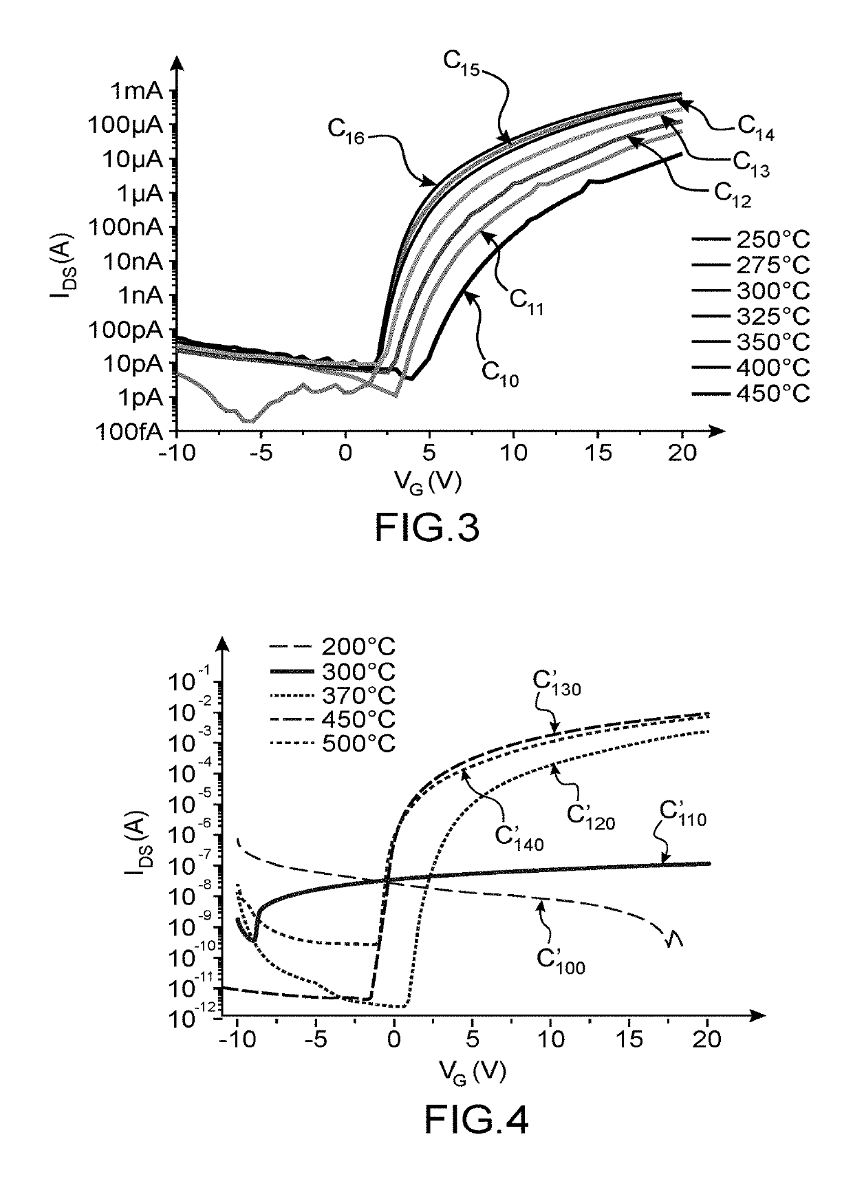
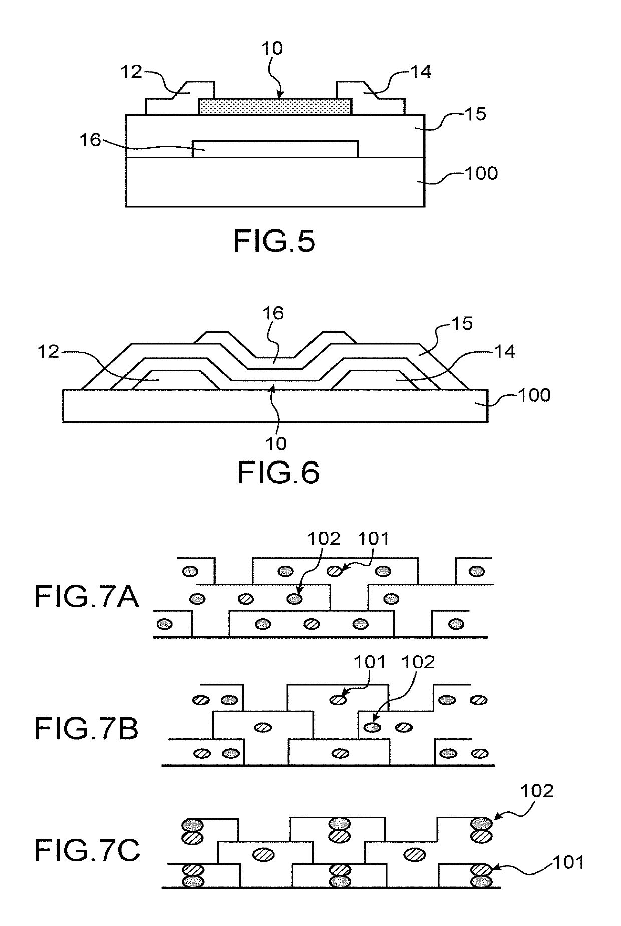
[0011]The inventors have discovered that the fact of producing a stack of metal oxide layers with atomic percentages of Zn, In and element X adapted and different from one layer to the next of the stack would make it possible to provide reduced annealing temperatures in order to make this stack active, and that an electronic component, in particular a transistor formed of such a material is functional, that is to say can follow different operating regimes (linear, saturated) and adopt different states (on, off) as a function of the manner in which it is biased.

[0012]The element X may be selected from the following elements: Ga, Sn, Sb, Be, Al, Ni.

[0013]According to one embodiment, the present invention relates to a method for forming on a substrate an active zone of metal oxide for an electronic device including:

[0014]a) liquid phase deposition on the substrate of a first solution based on indium, zinc and an element X selected from Ga, Sb, Be, Al, Ni, then heat treatment in such a ...


PUM

PropertyMeasurementUnit
temperatureaaaaaaaaaa
thicknessaaaaaaaaaa

Abstract

The present application relates to a method for forming an active zone of metal oxide for an electronic component including the formation of a stack of IXZO layers produced by liquid phase deposition on a substrate, the layers of said stack having different atomic fractions to each other in order to make it possible to reduce the annealing temperature enabling them to be made functional.

Description

TECHNICAL FIELD AND PRIOR ART[0001]The present application relates to the field of TFTs (thin film transistors), in particular those provided with an active layer based on metal oxide such as IGZO (indium gallium zinc oxide).[0002]As for a conventional transistor, in a TFT conduction takes place in a thin layer designated “active layer” between a source electrode and a drain electrode and in which the conductivity is modulated by a gate electrode.[0003]TFTs currently exist in which the active layer is based on hydrogenated amorphous silicon (a-Si:H) or polycrystalline silicon (poly-Si). TFTs in which the active layer is made of a metal oxide such as IGZO have also appeared. Such a material has the advantage of having a charge carrier mobility greater than that of amorphous silicon or polysilicon.[0004]A known technique for forming IGZO based layers is PVD (physical vapour deposition) and more specifically cathodic sputtering.[0005]Such a method requires the establishment of a high v...

Claims


Application Information

Patent Timeline
Patent Type & Authority Patents(United States)
IPC IPC(8): H01L21/02H01L29/24H01L29/786
CPCH01L21/02628H01L21/02422H01L21/02472H01L21/02483H01L21/02502H01L29/78693H01L21/02565H01L21/02592H01L21/02664H01L29/247H01L21/02554H01L29/66969H01L29/7869
Inventor BENWADIH, MOHAMMEDREVENANT-BRIZARD, CHRISTINE
Owner COMMISSARIAT A LENERGIE ATOMIQUE ET AUX ENERGIES ALTERNATIVES
Learn More