Method for continuously preparing organic light emitting diode by using thermal transfer film

a technology of thermal transfer film and organic light, which is applied in the direction of basic electric elements, electrical equipment, and semiconductor devices, etc., can solve the problems of long response time, bulky and heavy conventional cathode ray tube (crt) screen, and certain problems, and achieve low material efficiency

Active Publication Date: 2019-09-03
CHIEN HWA COATING TECH
View PDF16 Cites 1 Cited by
  • Summary
  • Abstract
  • Description
  • Claims
  • Application Information

AI Technical Summary

Benefits of technology

[0013]Therefore it is a primary object of the present invention to provide a method for continuously preparing organic light emitting diode (OLED) by using thermal transfer film in which at least two transfer layers on the thermal transfer film are heated and transferred onto a substrate in turn by thermal transfer printing for solving problems of complicated processes and low material efficiency of the conventional vacuum evaporation. Only less than 50% material reaches the substrate after the vacuum evaporation.

Problems solved by technology

A conventional Cathode Ray Tube (CRT) screen is bulky and heavy for users.
A longer response time is required at low temperature and liquid crystals can even freeze and cause performance problems.
However, certain problems occur during production processes of semiconductor products (such as OLED).
The method is difficult to scale because that highly accurate positioning of the metal mask is required and larger metal masks are easy to lose accuracy.
Thus the substrate used is limited to small scale one, difficult to scale up and unable to be mass produced.
The cost of the metal mask is extremely high and a cleaning process is required during production of the metal mask.
Furthermore, a lot of LOED materials are wasted during the vacuum evaporation.
The vacuum evaporation is simple but inefficient because only 10-40% material reaches the substrate after the process.

Method used


Image

  • Method for continuously preparing organic light emitting diode by using thermal transfer film
  • Method for continuously preparing organic light emitting diode by using thermal transfer film
  • Method for continuously preparing organic light emitting diode by using thermal transfer film

Examples


Embodiment Construction

[0043]In order to learn features and functions of the present invention, please refer to the following embodiments and the related descriptions.

[0044]In order to solve problems of the conventional vacuum evaporation used for preparing organic light emitting diode (OLED) (such as difficult scale-up and low material efficiency) that cause high production cost, a method for continuously preparing OLED by using thermal transfer film according to the present invention is provided.

[0045]The features, the structure of the method for continuously preparing OLED by using thermal transfer film according to the present invention are revealed by the following embodiments.

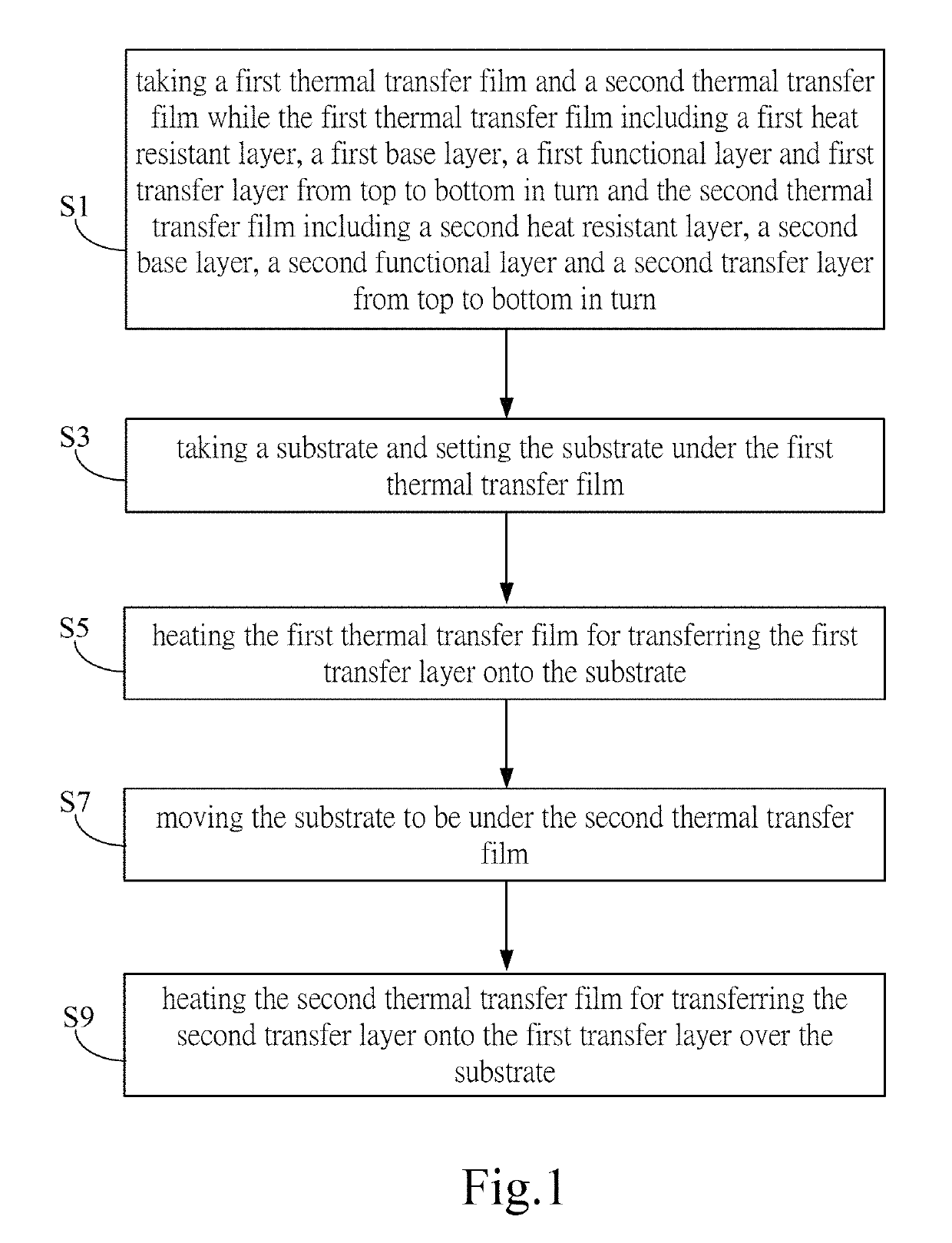
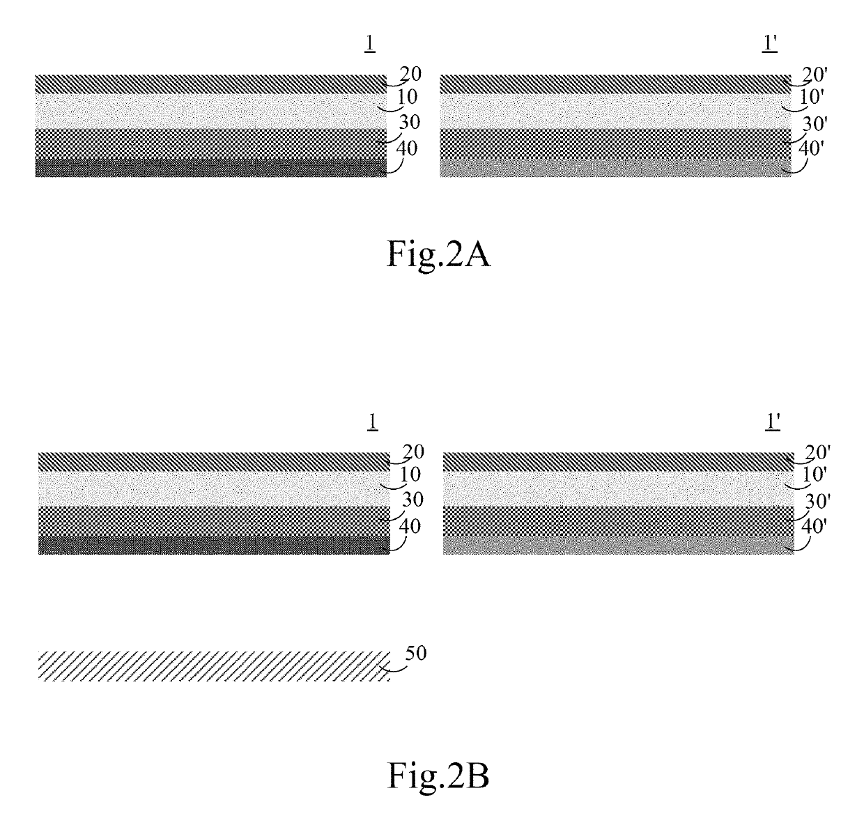
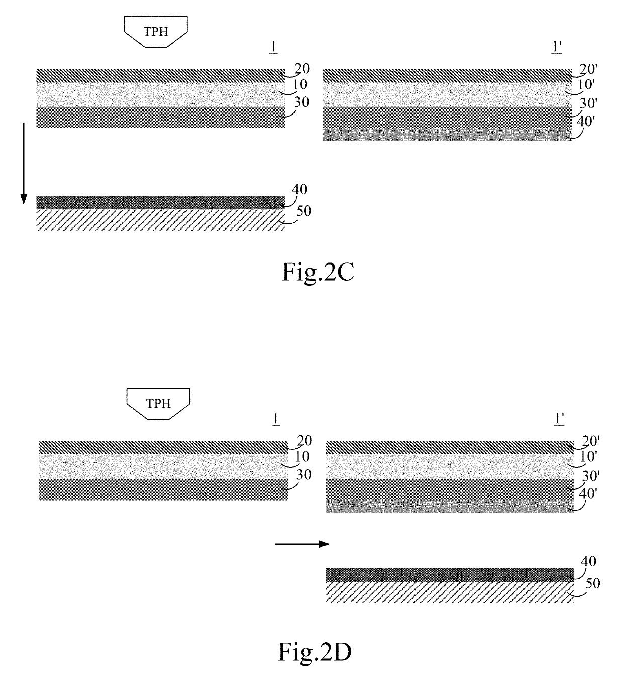
[0046]Refer to FIG. 1 and FIG. 2A-2E, a method for continuously preparing organic light emitting diode (OLED) by using thermal transfer film according to the present invention includes the following steps.[0047]S1: taking a first thermal transfer film and a second thermal transfer film while the first thermal transfer film incl...


PUM

PropertyMeasurementUnit
thicknessaaaaaaaaaa
thicknessaaaaaaaaaa
thicknessaaaaaaaaaa

Abstract

A method for continuously preparing organic light emitting diode (OLED) by using thermal transfer film is revealed. At least two thermal transfer layers are transferred onto a substrate in turn by thermal transfer printing for overcoming shortcomings of the conventional vacuum evaporation including complicated processes and low material efficiency. Only less than 50% material reaches the substrate after the vacuum evaporation.

Description

BACKGROUND OF THE INVENTIONField of the Invention[0001]The present invention relates to a method for preparing Organic Light Emitting Diode (OLED), especially to a method for continuously preparing organic light emitting diode (OLED) by using thermal transfer film.Description of Related Art[0002]A semiconductor is a kind of material whose electrical conductivity value falls between that of an insulator and a conductor. The semiconductor has a profound impact on either technology or economic development. The most common semiconductor materials include silicon, germanium, gallium arsenide, etc. The silicon is the most common and is used in the widespread commercial applications.[0003]Virtually all aspects of our lives are touched by semiconductor products. For example, Light-Emitting Diode (LED) and Laser Diode (LD) have been applied to illumination, indicator light sources, optical information storage system, laser printer, optical fiber communication and medical field, etc. Other pr...

Claims


Application Information

Patent Timeline
Patent Type & Authority Patents(United States)
IPC IPC(8): H01L51/00H01L51/52H01L51/56H01L51/50
CPCH01L51/5012H01L51/5206H01L51/529H01L51/56H01L51/0013H01L51/0026H01L51/5056H01L51/5072H01L51/5092H01L51/5221H10K71/18H10K50/00H10K71/00H10K50/11H10K50/15H10K50/16H10K50/81H10K50/82H10K50/87H10K50/171H10K71/40
Inventor SHIH, HUNG-HSIN
Owner CHIEN HWA COATING TECH
Why Eureka
Try Eureka