

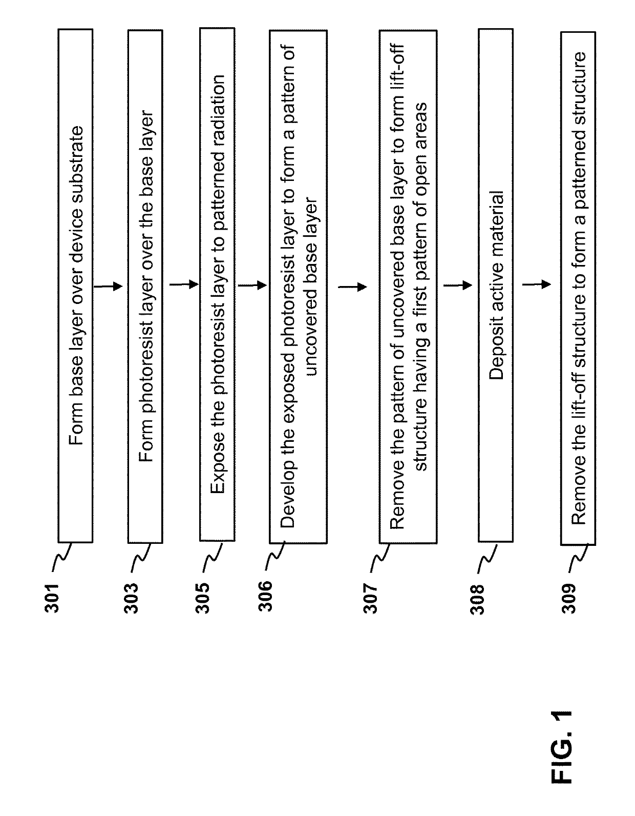
Photolithographic patterning of devices
a technology of photolithographic patterning and oled, which is applied in the direction of sustainable manufacturing/processing, instruments, final product manufacturing, etc., can solve the problems of deformation stress of masks, disadvantageous from the viewpoint of manufacturing costs, and the difficulty of position accuracy of mask openings, etc., to achieve high-efficiency lift-off resist systems, high resolution patterning, and easy use
- Summary
- Abstract
- Description
- Claims
- Application Information
AI Technical Summary
Benefits of technology
Problems solved by technology
Method used
Image

Examples
examples
[0127]Various fluorinated copolymers were prepared and their dissolution rates were measured in different hydrofluoroether solvents as models for the base layer developing agent and lift-off agent. Films were prepared by spin coating a target film on a silicon wafer followed by a post-apply bake at 90° C. for 1 min. Typical film thicknesses were 2 to 3 μm for this test. The rates were determined by measuring film thickness as a function of solvent contact lime using a Filmetrics F20 Thin Film Analyzer. This can be done either in situ or by applying the solvent of interest for set periods of time, spin drying and measuring the dry film. Rates greater than about 1000 nm / sec were generally too fast to measure accurately. Unless otherwise noted, all dissolution rates were conducted at room temperature, i.e., about 22° C.
[0128]Table 1 shows the rates for HFE-7100 (model lift-off agent) and HFE-7300 (model developing agent) wherein the copolymer included various amounts of a non-photoacti...
PUM
| Property | Measurement | Unit |
|---|---|---|
| temperature | aaaaa | aaaaa |
| temperature | aaaaa | aaaaa |
| temperature | aaaaa | aaaaa |
Abstract
Description
Claims
Application Information