
Semiconductor device manufacturing method and hard mask

a manufacturing method and semiconductor technology, applied in the direction of photomechanical equipment, instruments, originals for photomechanical treatment, etc., can solve the problems of affecting the alignment mark, the gate insulating film of the transistor may be subjected to dielectric breakdown, and the desired signal intensity may not be obtained, so as to prevent the charge-up phenomenon, prevent the dielectric breakdown of the semiconductor element, and facilitate the alignment

Inactive Publication Date: 2009-03-05
ELPIDA MEMORY INC
View PDF2 Cites 3 Cited by
  • Summary
  • Abstract
  • Description
  • Claims
  • Application Information

AI Technical Summary

Benefits of technology

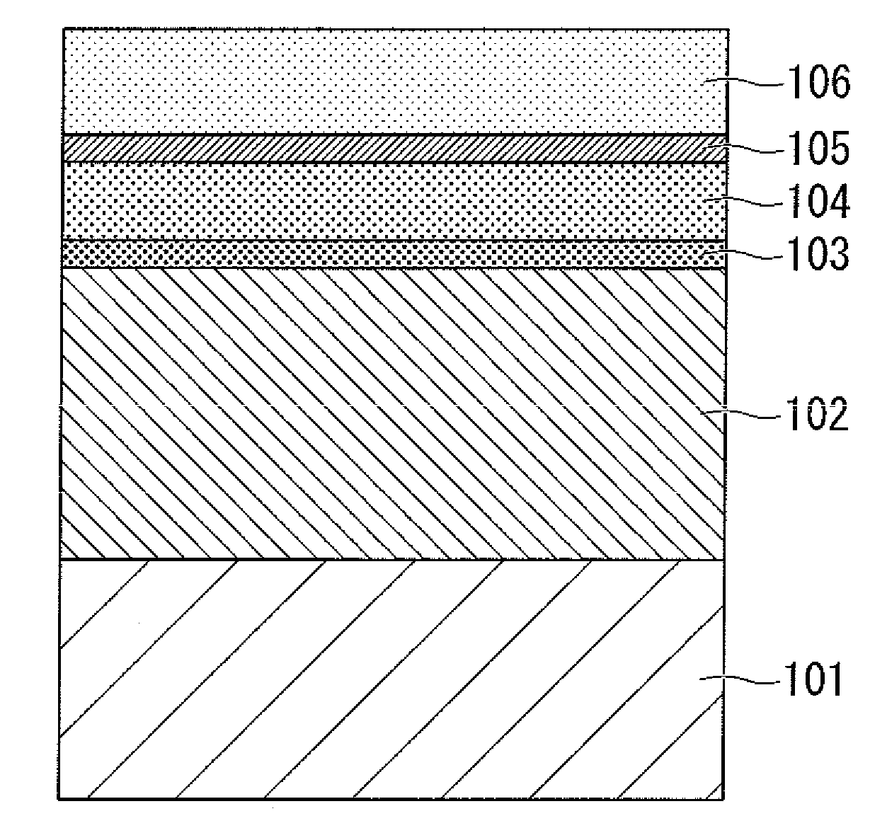
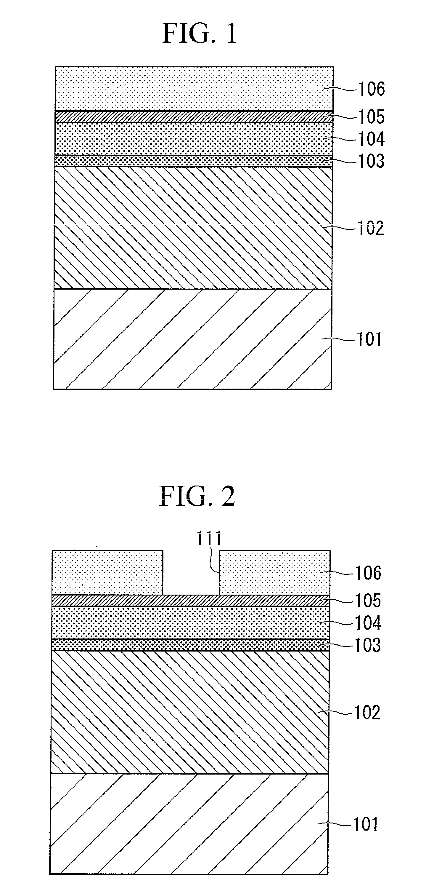
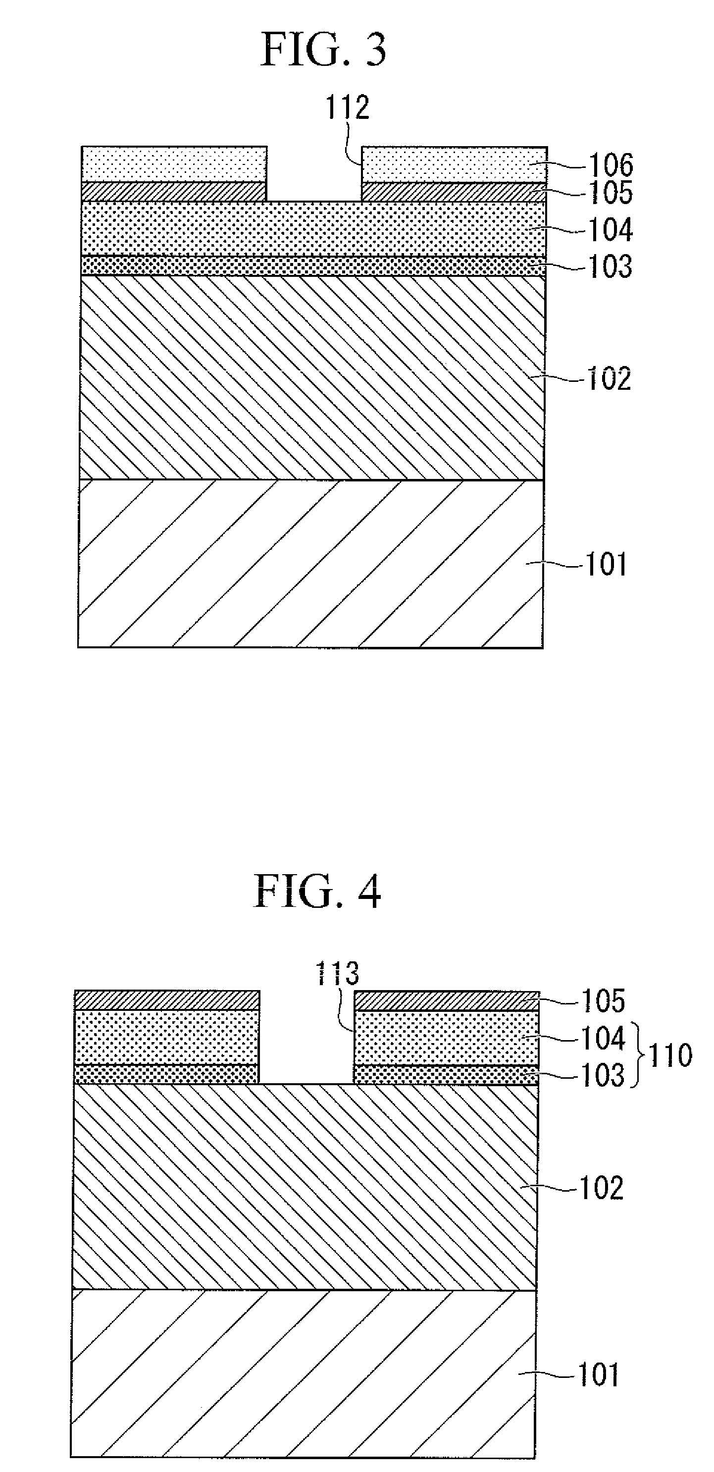
[0021]In accordance with the present invention in which the conductive carbon film is formed, it is possible to prevent a charge-up phenomenon of the hard mask and the semiconductor substrate, and thus to prevent dielectric breakdown of semiconductor elements on the semiconductor substrate. In addition, the transparent carbon film is also formed. Therefore, even when an alignment mark is formed below the hard mask, the alignment mark can be detected via the hard mask by using visible light. Accordingly, it is possible to easily perform alignment for the exposure when patterning the hard mask. Furthermore, as the hard mask is formed by carbon films, it can be used as an ashable hard mask.
[0022]Additionally, as a multilayer mask structure including the hard mask, the intermediate layer, and the resist layer is employed, high-resolution patterning is possible. For example, a contact hole having a high aspect ratio can be easily formed.

Problems solved by technology

When this potential difference increases, the gate insulating film of a transistor or the like, which has already been formed in a process prior to the process of forming the carbon film, may be subjected to dielectric breakdown.
Therefore, the present inventor recognized that a desired signal intensity from the alignment mark may not be obtained by simply forming a carbon film having a high conductivity, and that it may be difficult to provide etching resistivity to such a carbon film having a high conductivity, so as to use the carbon film as an ashable hard mask.

Method used


Image

  • Semiconductor device manufacturing method and hard mask
  • Semiconductor device manufacturing method and hard mask
  • Semiconductor device manufacturing method and hard mask

Examples


first example

[0071]A semiconductor device having a contact hole, as a first example, was manufactured as follows.

[0072]First, a silicon oxide film (i.e., a target film to be processed) was formed as an inter-layer insulating film on a semiconductor substrate in which a MOS transistor was formed. The MOS transistor had a gate insulating film which was a silicon oxide film having a thickness of 4 nm.

[0073]Next, a conductive carbon film was formed on the silicon oxide film provided on the semiconductor substrate. This film formation was performed using a PE-CVD apparatus (“Producer SE” manufactured by Applied Materials, Inc.), where the source gas was methane (CH4), and a specific high-temperature condition (called “APF (advanced patterning film)”) was employed, in which the temperature of a heater in the susceptor, on which the relevant heater is disposed, was set to 550° C., so that the film thickness would be 100 nm.

[0074]The resistivity of the formed conductive carbon film, which was measured u...


PUM

PropertyMeasurementUnit
thicknessaaaaaaaaaa
temperatureaaaaaaaaaa

Abstract

A semiconductor device manufacturing method includes forming a target film to be processed on a semiconductor substrate in which a semiconductor element has been formed; forming a hard mask on the target film; and patterning the target film. The hard mask is a multilayer film including a conductive carbon film and a transparent carbon film which are sequentially stacked on the target film. The formation of the hard mask may include sequentially stacking the conductive carbon film and the transparent carbon film on the target film on the semiconductor substrate; sequentially stacking an intermediate layer and a resist layer on the transparent carbon film; patterning the resist layer; patterning the intermediate layer by using the patterned resist layer as a mask; and patterning the conductive carbon film and the transparent carbon film by using the patterned intermediate layer as a mask.

Description

BACKGROUND OF THE INVENTION[0001]1. Field of the Invention[0002]The present invention relates to a method of manufacturing a semiconductor device, and also to a hard mask.[0003]Priority is claimed on Japanese Patent Application No. 2007-224423, filed Aug. 30, 2007, the contents of which are incorporated herein by reference.[0004]2. Description of Related Art[0005]Recently, when forming a contact hole having a high aspect ratio, or the like, a hard mask which can be easily removed by means of ashing (i.e., an ashable hard mask) has often been used. As such an ashable hard mask, a carbon film is used, which is formed by means of plasma-enhanced chemical vapor deposition (PE-CVD).[0006]Below, a known method of manufacturing a semiconductor device will be explained with reference to the drawings. FIGS. 7 to 12 are diagrams for showing processes of the manufacturing method in which a carbon film is used as an ashable hard mask.[0007]First, as shown in FIG. 7, on a semiconductor substrate...

Claims


Application Information

Patent Timeline
Patent Type & Authority Applications(United States)
IPC IPC(8): G03F1/00G03F7/20G03F7/40H01L21/027H01L21/28H01L21/285H01L21/3065H01L21/768
CPCG03F7/11H01L21/0332H01L21/76802H01L21/3146H01L21/31144H01L21/02115
Inventor HIROTA, TOSHIYUKI
Owner ELPIDA MEMORY INC
Learn More