
Methods and apparatus for forming submicron patterns on films

a technology of submicron patterns and films, applied in nanoinformatics, energy-based chemical/physical/physicochemical processes, nuclear engineering, etc., can solve the problems of limiting the performance of such integrated circuits, limiting the resolution of patterns, so as to achieve arbitrarily small lateral resolution of patterns

Inactive Publication Date: 2006-03-21
UNIV KONSTANZ +2
View PDF7 Cites 1 Cited by
  • Summary
  • Abstract
  • Description
  • Claims
  • Application Information

AI Technical Summary

Benefits of technology

[0016]The techniques disclosed herein can include many advantages, For example, the patterns are produced without optical radiation, and therefore their resolution is not limited by the wavelength of optical radiation. In principle the lateral resolution of the pattern can be made arbitrarily small by controlling the externally applied electric field and selecting a film with appropriate properties. Furthermore, the techniques can produce high-resolution patterns on the film without requiring the use of chemicals to etch or remove portions of the film.

Problems solved by technology

Limits on the resolution of such patterns limit the performance of such integrated circuits.
The resolution of the pattern is thus limited by the wavelength of light used to produce the optical pattern.

Method used


Image

  • Methods and apparatus for forming submicron patterns on films
  • Methods and apparatus for forming submicron patterns on films
  • Methods and apparatus for forming submicron patterns on films

Examples


example 1

Homogeneous Field

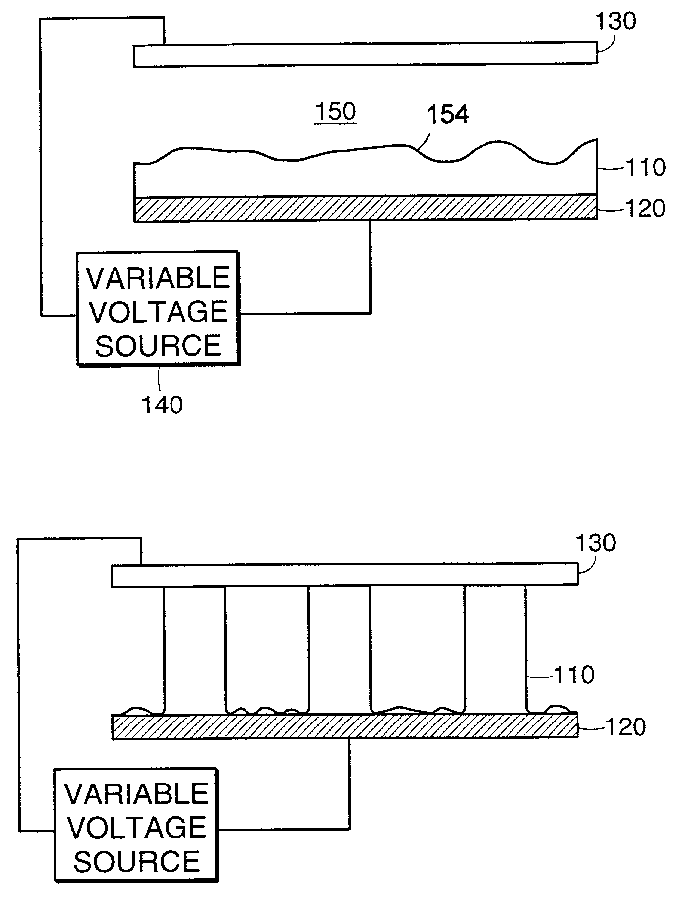
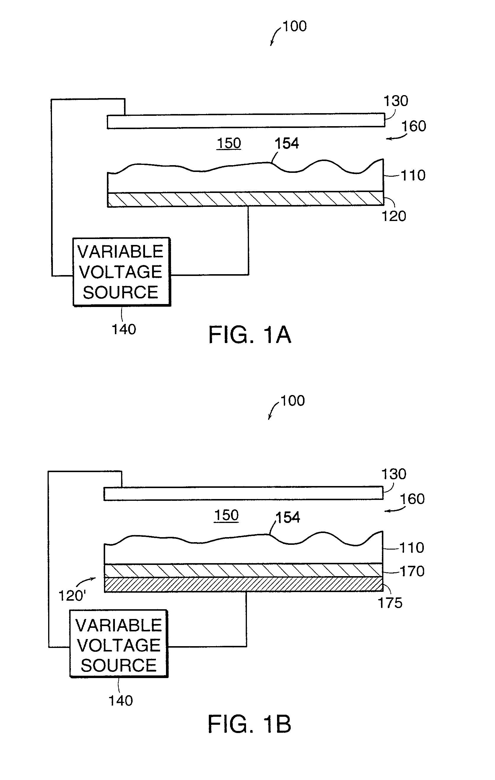
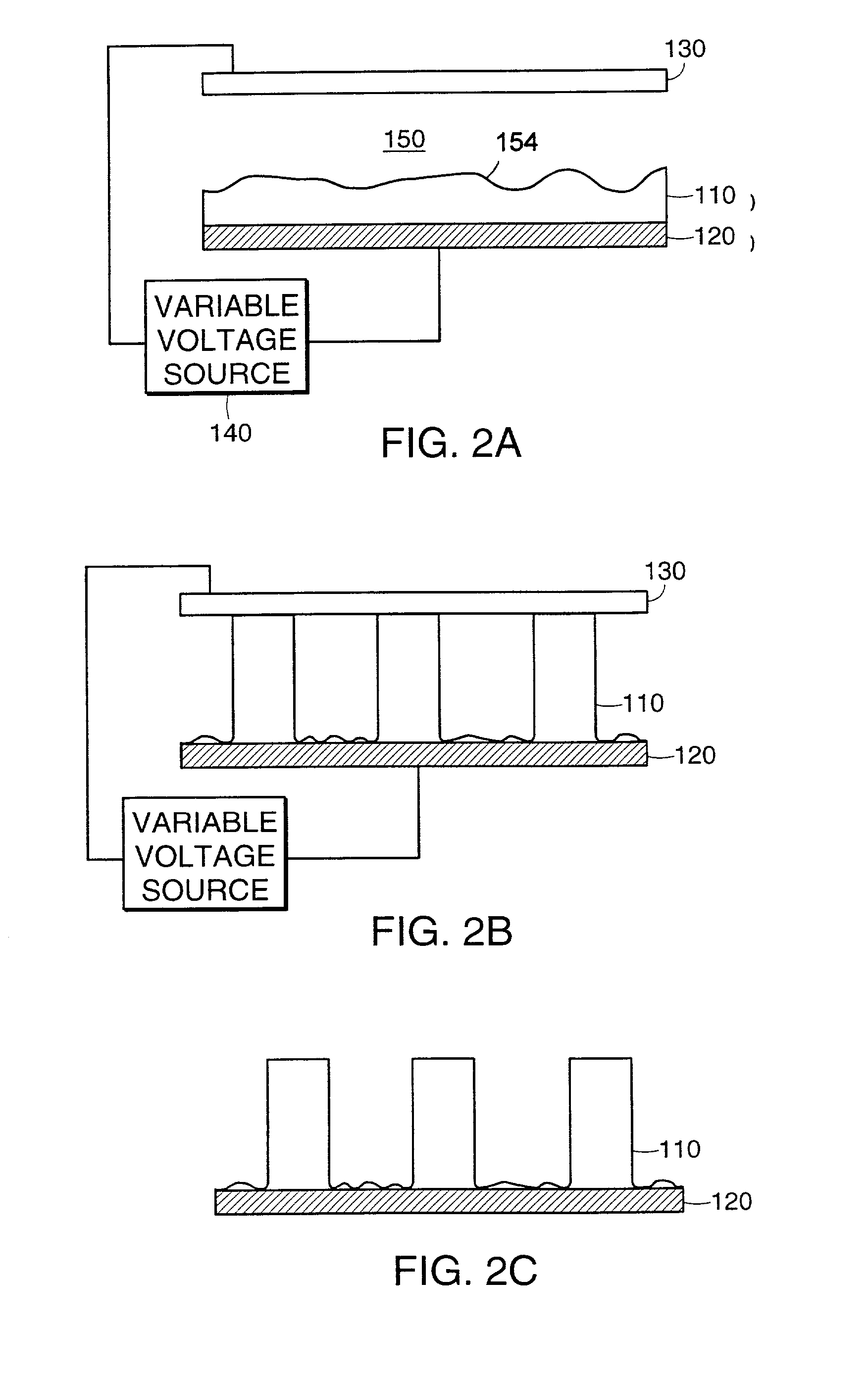
[0051]A thin polymer film of polystyrene (PS) of thickness h was spin-coated from solution onto a highly polished silicon wafer serving as one of the electrodes. Subsequently, another silicon wafer was mounted as the opposing electrode at a distance d leaving a thin air gap. The assembly was then heated above the glass transition temperature of the polymer (Tg) and a small voltage U (20–50 V) was applied. To assure the air gap, the top electrode had a small step. Using a wedge geometry a range of d values could be achieved, while locally maintaining a nearly parallel electrode configuration. Air gaps ranging from 100 nm to 1000 nm were achieved in this way. The voltage and the geometry of the capacitor device determine the electric field. The electrostatic driving force scales with the difference of the electric fields in the polymer film, Ep, and the air gap. Ep increases with decreasing values of d and increasing polymer film thickness h. The low applied voltage c...

example 2

Heterogeneous Fields

[0056]A patterned electrode was mounted facing a brominated polystyrene film (h˜45 nm), and the film was subjected to an applied voltage of 42 V. The device was maintained at 170° C. and exposed to the applied voltage for 20 hours. To ensure that no polymer remained on the master electrode after disassembly, the electrode was rendered unpolar by depositing of a self-assembled monolayer. FIG. 8 is an AFM image that shows 140 nm wide stripes (full-width half maximum), which replicate the silicon master electrode (200 nm stripes separated by 200 nm wide and 170 nm deep grooves). A cross-section measurement reveals a step height of 125 nm, with the resolution being limited by the geometry of the AFM tip. The profile of the polymer stripes is nearly rectangular with an aspect ratio of 0.83. The high quality of the replication extended over the entire 100×100 μm2 area that was covered by the master pattern.

example 3

Bilayer Liquids

[0057]Thin liquid films of polyisoprene (PI) and oligomeric styrene (OS) were spin-coated from toluene solutions onto bare and gold-coated silicon wafers, respectively. The film thickness was 140 nm. For some experiments a small air gap was left above the liquid to form liquid / air bilayers. In the remaining experiments, the air was replaced with a layer of oligomeric dimethylsiloxane (ODMS), thus forming a liquid / liquid bilayer. No solvent was used to deposit the ODMS layer. The overall thickness of the bilayer was nominally 1 μm. Table 1 below summarizes the physical constants of the liquid oligomers and polymers. From the scientific literature, the interfacial tension of OS / ODMS, OS / PI and PI / ODMS are 6.1 mN / m. 1.68 mN / m and 3.2 mN / m, respectively. Thin rails of silicon oxide were evaporated on top of indium-tin-oxide (ITO)-coated microscope slides (Delta Techologies), and these slides were mounted on top of the bilayer samples with the ITO and silicon oxide side fa...


PUM

PropertyMeasurementUnit
electric fieldaaaaaaaaaa
Laplace pressureaaaaaaaaaa

Abstract

A method for forming a patterned film on a substrate, the method including: providing a first flowable medium on the substrate and a second flowable medium on the first flowable medium, the first and second flowable media having different dielectric properties and defining an interface there between; applying an electric field to the interface for a time sufficient to produce a structure in the first flowable medium along the interface: and hardening the structure in the first flowable medium to form the patterned film.

Description

CROSS-REFERENCE TO RELATED APPLICATION[0001]This application is a continuation application of U.S. Ser. No. 09 / 746,667, field Dec. 22, 2000, U.S. Pat. No. 6,391,217, which claims benefit from U.S. provision application 60 / 173,001, filed on Dec. 23, 1999, which is incorporated herein by reference in its entirety.[0002]The invention relates to methods and apparatus for producing submicron patterns on films. This invention was made with government support under NSF #DMR-9809365. and DOE #DE-FG02-96ER45612. The government has certain rights in this invention.FIELD OF THE INVENTIONBackground of the Invention[0003]In the microelectronics, biotechnology, adhesive, and microsystem industries, it is important to produce high-resolution patterns on substrates. For examples, such high-resolution patterns are necessary to produce integrated circuits. Limits on the resolution of such patterns limit the performance of such integrated circuits. Presently, microlithography is commonly used to produ...

Claims


Application Information

Patent Timeline
Patent Type & Authority Patents(United States)
IPC IPC(8): B44C1/22B81C99/00G03F7/20G03F7/00H01L21/3105H05K3/00
CPCB82Y10/00B82Y40/00H01L21/31058G03F7/0002Y10T428/24521H05K3/0011H01L21/027
Inventor SCHAFFER, ERIKMLYNEK, JURGENSTEINER, ULLRICHTHURN-ALBRECHT, THOMASRUSSELL, THOMAS P.
Owner UNIV KONSTANZ
Learn More