Photoelectric conversion element and solid-state imaging apparatus

a technology of conversion elements and conversion elements, applied in the direction of solid-state devices, radiation controlled devices, semiconductor devices, etc., can solve problems such as reducing sensitivity

Active Publication Date: 2019-12-31
SONY SEMICON SOLUTIONS CORP
View PDF24 Cites 0 Cited by
  • Summary
  • Abstract
  • Description
  • Claims
  • Application Information

AI Technical Summary

Benefits of technology

[0010]Incidentally, a solid-state imaging apparatus is desired to have an excellent spectral shape in order to obtain an image having favorable color reproducibility. In addition, the solid-state imaging apparatus is desired to have response time speed (high responsivity) necessary for a photocurrent to rise or fall in response to turning on or off of light, and high external quantum efficiency (External Quantum Efficiency: EQE) for higher sensitivity.
[0011]It is desirable to provide a photoelectric conversion element that makes it possible achieve an excellent spectral shape, high responsivity, and high external quantum efficiency, and a solid-state imaging apparatus including the same.
[0014]In the photoelectric conversion element according to the embodiment of the present disclosure and the solid-state imaging apparatus according to the embodiment of the present disclosure, the photoelectric conversion layer is formed using the first organic semiconductor material and the second organic semiconductor material that have mutually different mother skeletons. Herein, the first organic semiconductor material is fullerene or the fullerene derivative, and the second organic semiconductor material has a deeper HOMO level than the first organic semiconductor material. This allows fullerene and the fullerene derivative to be used as a p-type semiconductor and makes it possible to improve hole mobility and electron mobility in the photoelectric conversion layer while maintaining a sharp spectral shape. This also makes it possible to enhance charge transport efficiency after excitons generated by light absorption are dissociated into charges.
[0015]According to the photoelectric conversion element of the embodiment of the present disclosure and the solid-state imaging apparatus of the embodiment of the present disclosure, the photoelectric conversion layer is formed using the first organic semiconductor material and the second organic semiconductor material described above, which makes it possible to obtain a sharp spectral shape, high charge mobility, and high charge transport efficiency. This makes it possible to provide a photoelectric conversion element having an excellent spectral shape, high responsivity, and high EQE, and a solid-state imaging apparatus including the same.

Problems solved by technology

In addition, in a case where a color filter including two-dimensionally arranged primary color filters of red, green, and blue is used for colorization, green light and blue light are absorbed by the color filter in a red pixel, for example, thus leading to the reduced sensitivity.

Method used


Image

  • Photoelectric conversion element and solid-state imaging apparatus
  • Photoelectric conversion element and solid-state imaging apparatus
  • Photoelectric conversion element and solid-state imaging apparatus

Examples


first embodiment (

1. First Embodiment (Example of a photoelectric conversion layer including three kinds of materials)

1-1. Configuration of Photoelectric Conversion Element

1-2. Method of Manufacturing Photoelectric conversion element

1-3. Workings and Effects

second embodiment (

2. Second Embodiment (Example of photoelectric conversion layer including two kinds of materials)

application examples

3. Application Examples

4. Examples

1. First Embodiment

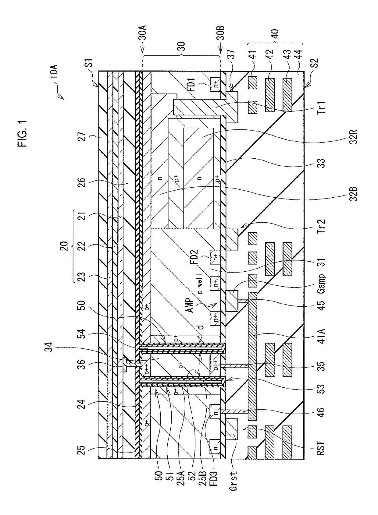
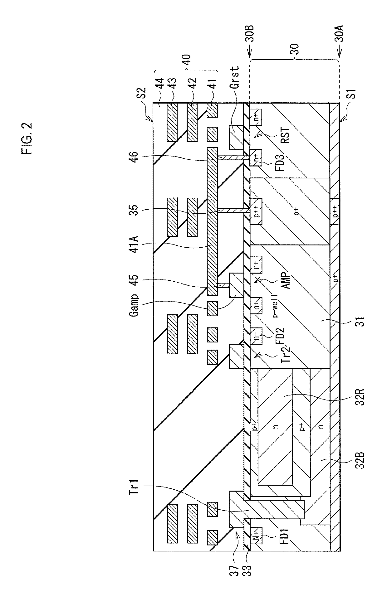
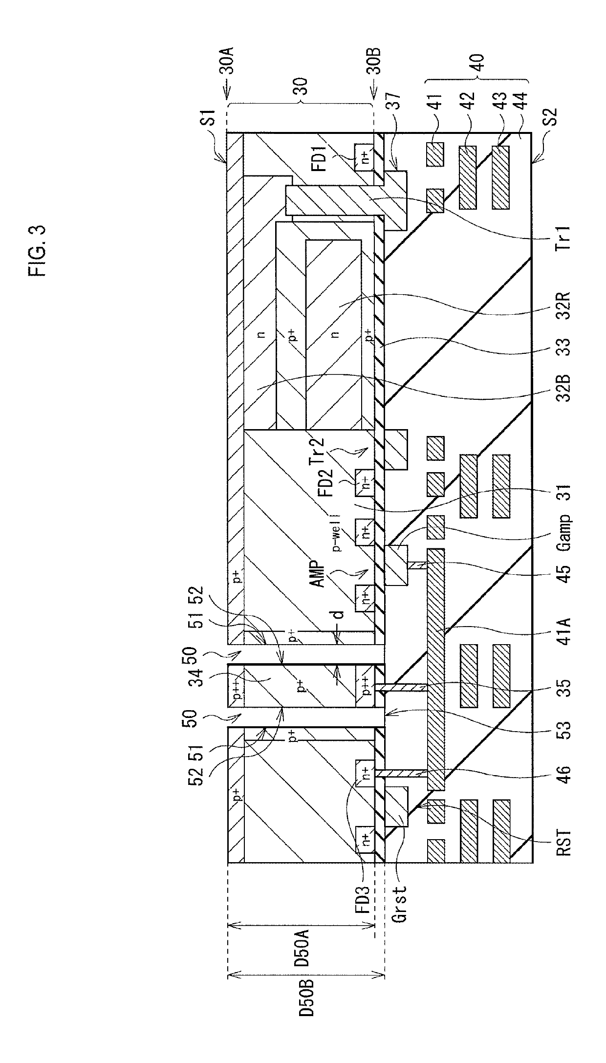
[0029]FIG. 1 illustrates a cross-sectional configuration of a photoelectric conversion element (a photoelectric conversion element 10A) according to a first embodiment of the present disclosure. The photoelectric conversion element 10A configures a pixel (a unit pixel P) in a solid-state imaging apparatus (a solid-state imaging apparatus 1: see FIG. 7) such as a CMOS image sensor used in an electronic apparatus such as a digital still camera, or a video camera, for example.

1-1. Configuration of Photoelectric Conversion Element

[0030]The photoelectric conversion element 10A is of a so-called longitudinal spectral type in which, for example, one organic photoelectric converter 20 and two inorganic photoelectric converters 32B and 32R are stacked in a longitudinal direction. The organic photoelectric converter 20 is provided on a side on which a first surface (back side) 30A is located of a semiconductor substrate 30. The inorganic ph...


PUM


Abstract

A photoelectric conversion element according to an embodiment of the present disclosure includes a first electrode and a second electrode opposed to each other; and a photoelectric conversion layer provided between the first electrode and the second electrode, and including a first organic semiconductor material and a second semiconductor material that have mutually different mother skeletons, in which the first organic semiconductor material is fullerene or a fullerene derivative, and the second organic semiconductor material has a deeper HOMO level than the first organic semiconductor material.

Description

CROSS REFERENCE TO RELATED APPLICATIONS[0001]This application is a national stage application under 35 U.S.C. 371 and claims the benefit of PCT Application No. PCT / JP2017 / 021262 having an international filing date of 8 Jun. 2017, which designated the United States, which PCT application claimed the benefit of Japanese Patent Application No. 2016-142547 filed 20 Jul. 2016, the entire disclosures of each of which are incorporated herein by reference.TECHNICAL FIELD[0002]The present disclosure relates to a photoelectric conversion element using an organic semiconductor material, for example, and a solid-state imaging apparatus including the same.BACKGROUND ART[0003]In recent years, in a solid-state imaging apparatus such as a CCD (Charge Coupled Device) image sensor or a CMOS (Complementary Metal Oxide Semiconductor) image sensor, miniaturization of pixel size has been under way. This causes a reduction in the number of photons entering a unit pixel, thus resulting in reduced sensitivi...

Claims


Application Information

Patent Timeline
Patent Type & Authority Patents(United States)
IPC IPC(8): H01L51/42H01L27/30H01L27/146H01L31/10H01L27/28H01L51/00
CPCH01L51/4253H01L27/286H01L27/30H01L27/307H01L51/4206H01L31/10H01L27/146H01L51/424H01L27/301H01L51/42H01L51/0078H01L51/0046H01L51/0053H01L51/0072H01L51/0073H01L51/0047H01L51/008Y02E10/549H10K85/211H10K85/215H10K85/6574H10K85/322H10K85/6572H10K30/30H10K30/00H10K19/20H10K30/20H10K30/451H10K39/00H10K39/10H10K39/32H10K85/311H10K85/621
Inventor MATSUZAWA, NOBUYUKIHASEGAWA, YUTAOBANA, YOSHIAKITAKEMURA, ICHIROYAMAGUCHI, TETSUJIENOKI, OSAMU
Owner SONY SEMICON SOLUTIONS CORP
Why Eureka
Try Eureka