Electro-optical device and electronic apparatus

a technology of optical devices and electronic devices, applied in the direction of capacitors, structural fixed capacitor combinations, instruments, etc., can solve the problems of inability to hold potential applied to the pixel electrode, difficult to ensure the electric capacitance of the holding capacitor, and the inability to ensure the holding capacitor. , to achieve the effect of stabilizing the driving state and suppressing the occurren

Active Publication Date: 2020-02-18
SEIKO EPSON CORP
View PDF12 Cites 0 Cited by
  • Summary
  • Abstract
  • Description
  • Claims
  • Application Information

AI Technical Summary

Benefits of technology

[0008]According to the application example, since the second electrode layer constituting the first capacitance electrode contains silicide of a metal more stabilized through silicidation than tungsten, the second electrode layer is more thermally stabilized than the first electrode layer containing tungsten silicide. In addition, the third electrode layer containing silicon is stacked on the second electrode layer. Accordingly, even when a high temperature treatment at, for example, 600° C. or greater is performed in forming the transistor or the like, silicidation proceeds owing to the heat applied to the second electrode layer, and silicon becomes difficult to liberate. For this reason, a defect of a reduction of a light shielding property or physical strength due to a change in film quality of the second electrode layer caused by the high temperature treatment can be prevented. In other words, as compared to a case where the first capacitance electrode includes only the first electrode layer containing tungsten silicide, a reduction of a light shielding property of the first capacitance electrode can be suppressed even when a high temperature treatment is performed. Additionally, the third electrode layer contains silicon and thus, in forming the capacitance insulation film including a silicon oxide film or a silicon nitride film on the third electrode layer, the third electrode layer becomes less susceptible to influence of the metal element incorporated in the second electrode layer, and a high insulation property can be ensured in the capacitance insulation film. Namely, the electro-optical device capable of blocking incident light by the first capacitance electrode constituting the holding capacitor even when the light is incident from the substrate side toward the transistor, and including the holding capacitor having desired electric capacitance can be provided.
[0034]According to the application example, the electronic apparatus capable of blocking light incident from the substrate side toward the transistor by the holding capacitor and thus, capable of suppressing occurrence of a light leakage current in the transistor to realize a stabilized driving state can be provided.

Problems solved by technology

In pixels having high definition to achieve high-quality image display, the area in which the holding capacitor can be provided in each pixel reduces and thus, it becomes difficult to ensure a holding capacitor having desired electric capacitance.
When the electric capacitance of the holding capacitor reduces, the potential applied to the pixel electrode cannot be held for predetermined time, and a defect in display such as flickering is caused.
Similarly, in a case where the electrode is formed by using silicide of a metal, when a high temperature treatment is performed, silicon is liberated from the silicide of the metal and film quality changes, and again, a light shielding property may reduce or physical strength may decrease.
Accordingly, depending on disposition of an electro-optical device with respect to a light source, when the light is incident from the substrate side toward the transistor and a light shielding property of the holding capacitor is reduced, the light is incident on the transistor to cause a light leakage current, and there has been an issue of a potential of a pixel electrode that cannot be switch-controlled stably.
Accordingly, even when a high temperature treatment at, for example, 600° C. or greater is performed in forming the transistor or the like, silicidation proceeds owing to the heat applied to the second electrode layer, and silicon becomes difficult to liberate.
Accordingly, a change in film quality of the second electrode layer due to the heat used in forming the capacitance insulation film becomes difficult to occur, and a reduction of the light shielding property of the first capacitance electrode is suppressed.

Method used


Image

  • Electro-optical device and electronic apparatus
  • Electro-optical device and electronic apparatus
  • Electro-optical device and electronic apparatus

Examples


first exemplary embodiment

Electro-Optical Device

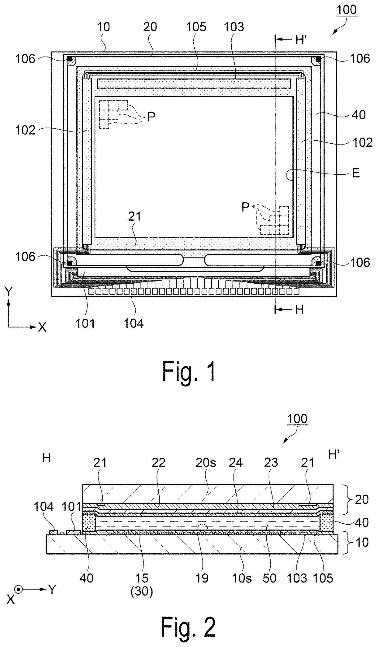
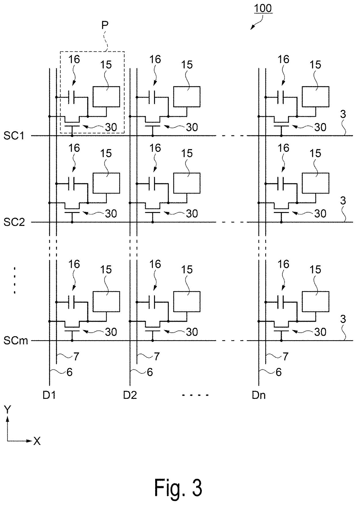
[0066]First, a configuration of a liquid crystal device as an electro-optical device according to a first exemplary embodiment will be described with reference to FIGS. 1 to 3. FIG. 1 is a schematic plan view illustrating a configuration of a liquid crystal device as an electro-optical device according to the first exemplary embodiment, FIG. 2 is a schematic cross-sectional view taken along line H-H′ of the liquid crystal device illustrated in FIG. 1, and FIG. 3 is an equivalent circuit diagram illustrating an electrical configuration of the liquid crystal device according to the first exemplary embodiment.

[0067]As illustrated in FIG. 1 and FIG. 2, a liquid crystal device 100 of the first exemplary embodiment includes an element substrate 10 and a counter substrate 20 disposed to face each other, and a liquid crystal layer 50 interposed between a pair of these substrates. For example, a quartz substrate or a glass substrate having a translucent property is used...

second exemplary embodiment

Electro-Optical Device

[0151]Next, an electro-optical device of the second exemplary embodiment will be described by exemplifying a liquid crystal device as with the first exemplary embodiment. The liquid crystal device as the electro-optical device of the second exemplary embodiment includes a liquid crystal layer interposed between an element substrate and a counter substrate, and is different from the first exemplary embodiment in disposition of a scanning line and a holding capacitor between a base substrate 10s and a TFT 30 in the element substrate and a configuration related to each of the scanning line and the holding capacitor. Accordingly, the same configurations as the configurations in the liquid crystal device 100 of the first exemplary embodiment are denoted by the same reference signs, and detailed description of the same configurations will be omitted.

[0152]FIG. 22 is a schematic plan view illustrating disposition of the TFT, wiring, and the like at an intersection of ...

third exemplary embodiment

Electronic Apparatus

[0204]Next, a projection-type display apparatus will be described with reference to FIG. 28 as an example of an electronic apparatus to which the liquid crystal device according to each of the above-described embodiments is applied. FIG. 28 is a schematic view illustrating a configuration of the projection-type display apparatus as the electronic apparatus.

[0205]As illustrated in FIG. 28, a projection-type display apparatus 1000 as an electronic apparatus according to a third exemplary embodiment includes a polarized light illumination apparatus 1100 disposed along a system optical axis L, and two dichroic mirrors 1104 and 1105 as light separation elements. In addition, the projection-type display apparatus 1000 includes three reflection mirrors 1106, 1107 and 1108 and five relay lenses 1201, 1202, 1203, 1204, and 1205. Further, the projection-type display apparatus 1000 includes liquid crystal light bulbs 1210, 1220, and 1230 of a transmissive type as three ligh...


PUM

PropertyMeasurementUnit
temperatureaaaaaaaaaa
thicknessaaaaaaaaaa
thicknessaaaaaaaaaa

Abstract

A liquid crystal device as an electro-optical device includes a base substrate as a substrate, a TFT as a transistor, and a holding capacitor, and the holding capacitor includes a first capacitance electrode disposed on the base substrate side and a second capacitance electrode disposed on the first capacitance electrode via a capacitance insulation film, and the first capacitance electrode includes a first electrode layer containing tungsten silicide, a second electrode layer containing silicide of a metal more stabilized through silicidation than tungsten, and a third electrode layer containing silicon stacked one on another.

Description

BACKGROUND1. Technical Field[0001]The disclosure relates to an electro-optical device and an electronic apparatus including the electro-optical device.2. Related Art[0002]As an electro-optical device, for example, an active drive type liquid crystal device including a transistor capable of switch-controlling a potential of a pixel electrode for each pixel is known. In such a liquid crystal device, a holding capacitor configured to hold the potential applied to the pixel electrode is provided for each pixel. In pixels having high definition to achieve high-quality image display, the area in which the holding capacitor can be provided in each pixel reduces and thus, it becomes difficult to ensure a holding capacitor having desired electric capacitance. When the electric capacitance of the holding capacitor reduces, the potential applied to the pixel electrode cannot be held for predetermined time, and a defect in display such as flickering is caused.[0003]To address such a defect rela...

Claims


Application Information

Patent Timeline
Patent Type & Authority Patents(United States)
IPC IPC(8): G02F1/1362G09G3/36H01L49/02H01G4/005
CPCH01L28/60G02F1/136213G09G3/3648H01G4/005H01G4/40G02F1/136209G02F1/136286G02F1/13685G02F1/13629G02F1/136295
Inventor KAWATA, HIDENORI
Owner SEIKO EPSON CORP
Why Eureka
Try Eureka