Preparation method of flexible transparent circuit
a flexible transparent circuit and manufacturing method technology, applied in the direction of circuit bendability/stretchability, dielectric characteristics, conductive pattern formation, etc., can solve the problems of easy breakage of films, difficult to precisely control the quality of graphene films, and tendency to form wrinkles, etc., to achieve excellent properties of stretch, bending and twisting, good conductivity
- Summary
- Abstract
- Description
- Claims
- Application Information
AI Technical Summary
Benefits of technology
Problems solved by technology
Method used
Image

Examples
embodiment 1
[0033]The silver nanowire (AgNWs) ethanol solution used in the present invention has the following specifications: a diameter of 30 nm, a length of 100 to 200 um, a concentration of 20 mg / ml and a solvent of the anhydrous ethanol.
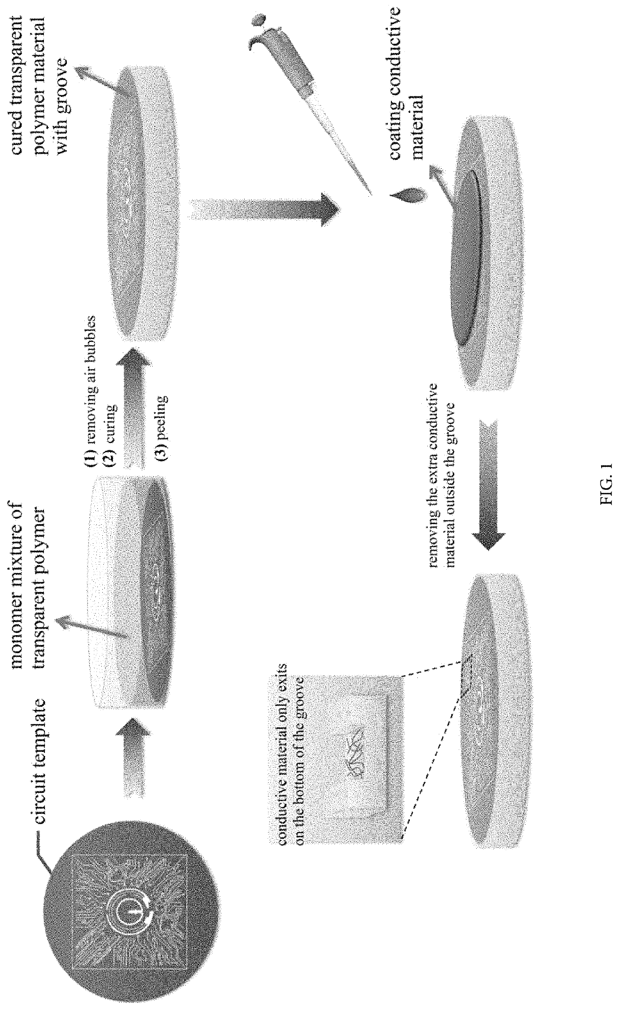
1. Preparing the Circuit Template
[0034]With the photolithographic technology, a circuit having a protruding surface structure is patterned on a silicon wafer of 4 inch by using the SU-2050 photoresist to form the circuit template.
2. Preparing the PDMS Transparent Carrier
[0035]The liquid A and liquid B of the Polydimethylsiloxane (Polydimethylsiloxane, PDMS) are mixed uniformly in a ratio of 10:1. Then the mixture is poured on the template prepared with the silicon wafer that is patterned a circuit pattern. The air bubbles in the PDMS are removed in the vacuum dryer. The drying time is around 1 hour. Later, the template is placed in an oven at 80° C. to be cured and heated for 1 hour to eventually form the cured transparent PDMS carrier having the groove cir...
embodiment 2
[0039]The copper nanowire (CuNWs) ethanol solution used in the present invention has the following specifications: a diameter of 20 nm, a length of 80 um, a concentration of 20 mg / ml and a solvent of the anhydrous ethanol.
1. Preparing the Circuit Template
[0040]With the photolithographic technology, a desired circuit is patterned on a silicon wafer of 4 inch by using the SU-2050 photoresist to form the template.
2. Preparing the PDMS Transparent Carrier
[0041]The liquid A and liquid B of the Polydimethylsiloxane (Polydimethylsiloxane, PDMS) are mixed uniformly in a ratio of 10:1. Then the mixture is poured on the template prepared with the silicon wafer that is patterned a circuit pattern. The air bubbles in the PDMS are removed in the vacuum dryer. The drying time is around 1hour. Later, the template is placed in an oven at 80° C. to be cured and heated for 1 hour to eventually form the cured transparent PDMS carrier having the groove circuit structure.
3. Preparing the Flexible Transp...
embodiment 3
[0045]The gold nanowire (AuNWs) ethanol solution used in the present invention has the following specifications: a diameter of 3 nm, a length of 50 um, a concentration of 20 mg / ml and a solvent of the anhydrous ethanol.
1. Preparing the Circuit Template
[0046]With the photolithographic technology, a desired circuit is patterned on a silicon wafer of 4 inch by using the SU-2050 photoresist to form the template.
2. Preparing the PDMS Transparent Carrier
[0047]The liquid A and liquid B of the Polydimethylsiloxane (Polydimethylsiloxane, PDMS) are mixed uniformly in a ratio of 10:1. Then the mixture is poured on the mould prepared with the silicon wafer that is patterned a circuit pattern. The air bubbles in the PDMS are removed in the vacuum dryer. The drying time is around 1 hour. Later, the template is placed in an oven at 80° C. to be cured and heated for 1 hour to eventually form the cured transparent PDMS carrier having the groove circuit structure.
3. Preparing the Flexible Transparent...
PUM
| Property | Measurement | Unit |
|---|---|---|
| transparency | aaaaa | aaaaa |
| concentration | aaaaa | aaaaa |
| length | aaaaa | aaaaa |
Abstract
Description
Claims
Application Information
 - R&D
- Intellectual Property
- Life Sciences
- Materials
- Tech Scout
- Unparalleled Data Quality
- Higher Quality Content
- 60% Fewer Hallucinations
Browse by: Latest US Patents, China's latest patents, Technical Efficacy Thesaurus, Application Domain, Technology Topic, Popular Technical Reports.
© 2025 PatSnap. All rights reserved.Legal|Privacy policy|Modern Slavery Act Transparency Statement|Sitemap|About US| Contact US: help@patsnap.com