Preparation method of flexible transparent circuit

Active Publication Date: 2020-01-16
DALIAN UNIVERSITY
View PDF3 Cites 2 Cited by
  • Summary
  • Abstract
  • Description
  • Claims
  • Application Information

AI Technical Summary

Benefits of technology

[0009]In order to make up the blank in the prior art, the present invention discloses a manufacturing method of a flexible transparent material. Both the substrate and the circuit conductive part of the flexible transparent circuit manufactured by such method are transparent, which realizes a t

Problems solved by technology

1. The graphene films, especially the graphene films having a large area, tend to form wrinkles;
2. The precise control of the quality for the graphene films is difficult to proceed, and the films get broken easily;
3. The mass production of the graphene films is hard to carry out;
4. The best graphene film has a sheet resistance of around 100 Ohms, and the transparency thereof is only 90%.
However, such method has a complicated process and an inaccurate circuit control.
And the circuit cannot have a

Method used


Image

  • Preparation method of flexible transparent circuit
  • Preparation method of flexible transparent circuit
  • Preparation method of flexible transparent circuit

Examples


embodiment 1

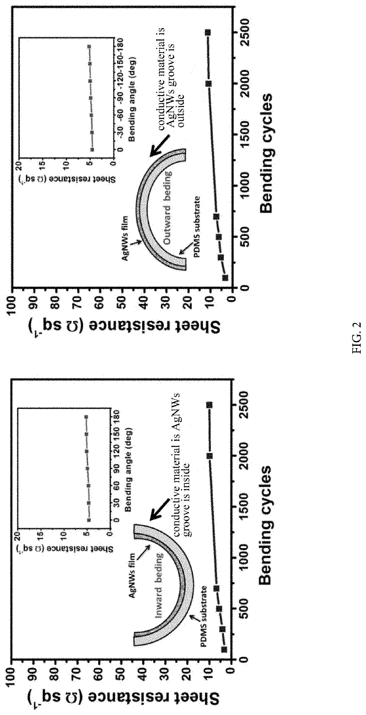
[0033]The silver nanowire (AgNWs) ethanol solution used in the present invention has the following specifications: a diameter of 30 nm, a length of 100 to 200 um, a concentration of 20 mg / ml and a solvent of the anhydrous ethanol.

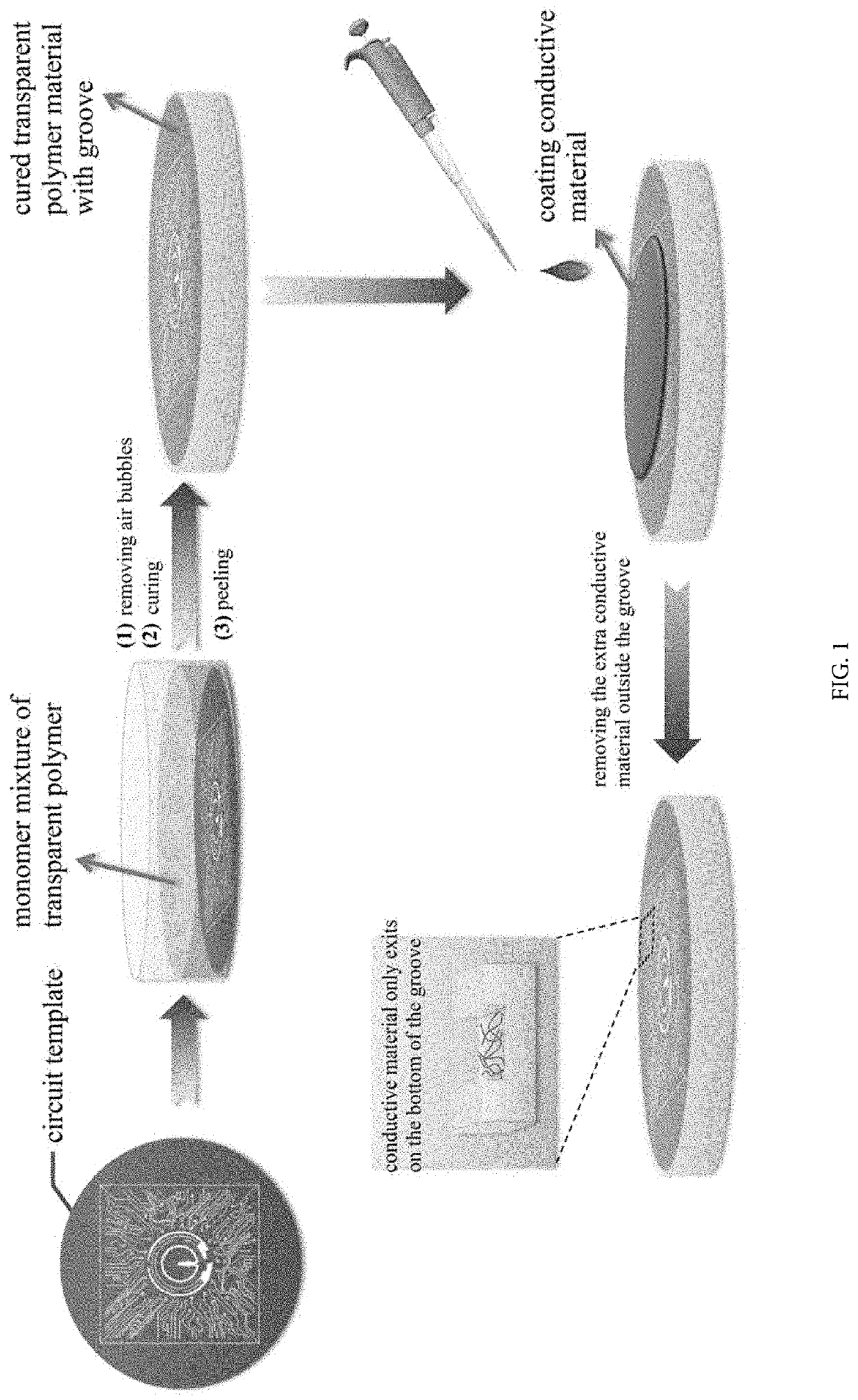
[0034]1. Preparing the Circuit Template

[0035]With the photolithographic technology, a circuit having a protruding surface structure is patterned on a silicon wafer of 4 inch by using the SU-2050 photoresist to form the circuit template.

[0036]2. Preparing the PDMS Transparent Carrier

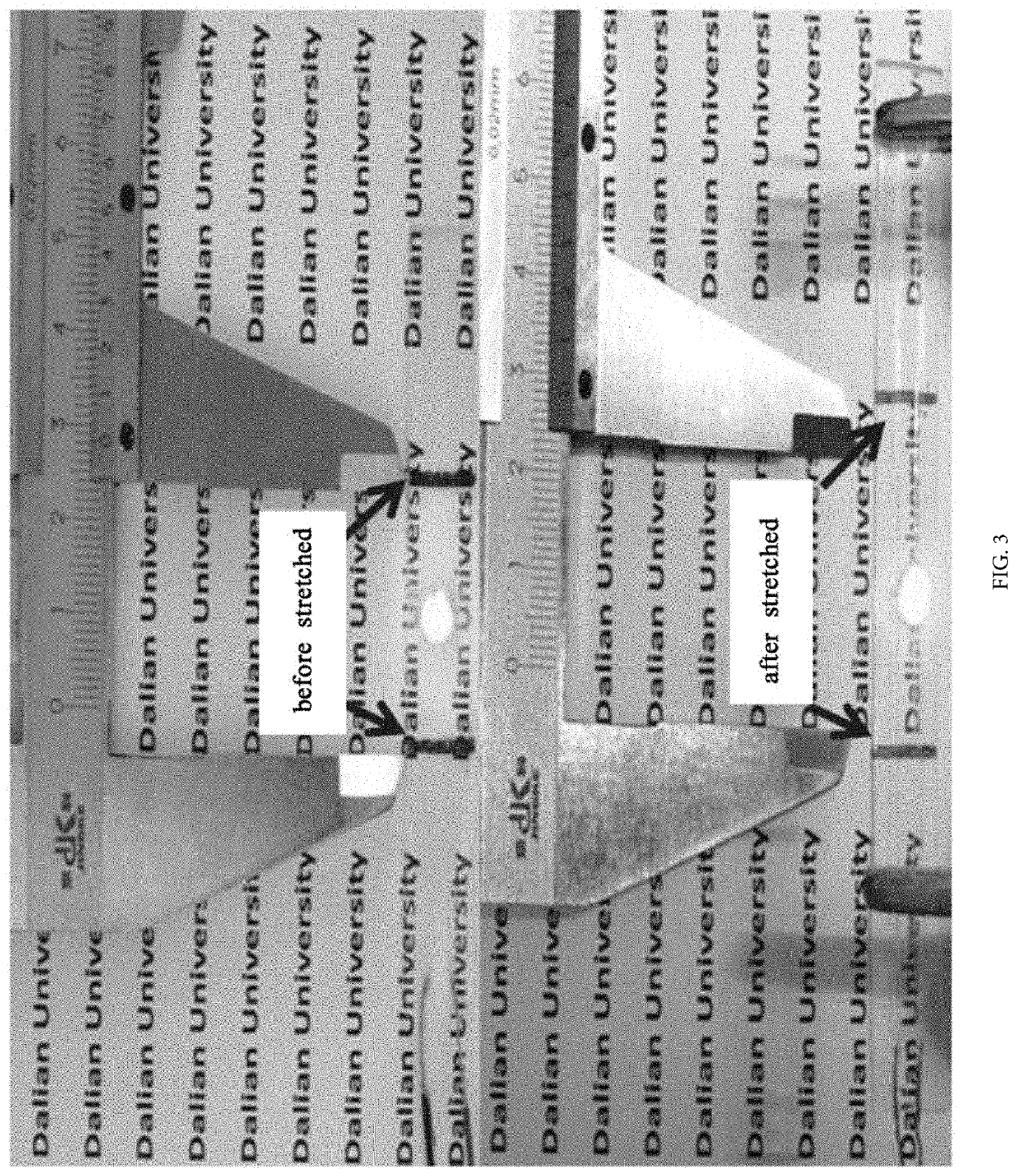
[0037]The liquid A and liquid B of the Polydimethylsiloxane (Polydimethylsiloxane, PDMS) are mixed uniformly in a ratio of 10:1. Then the mixture is poured on the template prepared with the silicon wafer that is patterned a circuit pattern. The air bubbles in the PDMS are removed in the vacuum dryer. The drying time is around 1 hour. Later, the template is placed in an oven at 80° C. to be cured and heated for 1 hour to eventually form the cured transparent PDMS carrier having th...

embodiment 2

[0042]The copper nanowire (CuNWs) ethanol solution used in the present invention has the following specifications: a diameter of 20 nm, a length of 80 um, a concentration of 20 mg / ml and a solvent of the anhydrous ethanol.

[0043]1. Preparing the Circuit Template

[0044]With the photolithographic technology, a desired circuit is patterned on a silicon wafer of 4 inch by using the SU-2050 photoresist to form the template.

[0045]2. Preparing the PDMS Transparent Carrier

[0046]The liquid A and liquid B of the Polydimethylsiloxane (Polydimethylsiloxane, PDMS) are mixed uniformly in a ratio of 10:1. Then the mixture is poured on the template prepared with the silicon wafer that is patterned a circuit pattern. The air bubbles in the PDMS are removed in the vacuum dryer. The drying time is around 1 hour. Later, the template is placed in an oven at 80° C. to be cured and heated for 1 hour to eventually form the cured transparent PDMS carrier having the groove circuit structure.

[0047]3. Preparing ...

embodiment 3

[0051]The gold nanowire (AuNWs) ethanol solution used in the present invention has the following specifications: a diameter of 3 nm, a length of 50 um, a concentration of 20 mg / ml and a solvent of the anhydrous ethanol.

[0052]1. Preparing the Circuit Template

[0053]With the photolithographic technology, a desired circuit is patterned on a silicon wafer of 4 inch by using the SU-2050 photoresist to form the template.

[0054]2. Preparing the PDMS Transparent Carrier

[0055]The liquid A and liquid B of the Polydimethylsiloxane (Polydimethylsiloxane, PDMS) are mixed uniformly in a ratio of 10:1. Then the mixture is poured on the mould prepared with the silicon wafer that is patterned a circuit pattern. The air bubbles in the PDMS are removed in the vacuum dryer. The drying time is around 1 hour. Later, the template is placed in an oven at 80° C. to be cured and heated for 1 hour to eventually form the cured transparent PDMS carrier having the groove circuit structure.

[0056]3. Preparing the Fl...


PUM

PropertyMeasurementUnit
Flexibilityaaaaaaaaaa
Electrical conductoraaaaaaaaaa
Transparencyaaaaaaaaaa

Abstract

A manufacturing method of a flexible transparent circuit includes preparing a circuit template. The method further includes using a flexible transparent polymer material to prepare a cured transparent carrier on the circuit template, wherein the cured transparent carrier has a groove circuit structure. The method includes coating a solution containing a conductive material in a groove of the cured transparent carrier. The method further includes forming a circuit with the high transparency and conductivity after the solvent is volatilized. The circuit are designed and manufactured according to the requirements, and the precision thereof is able to achieve the micron or nanometer level. The formed circuit is light. The circuit can be stretched, bended or twisted many times. The circuit has a good biological compatibility. The circuit manufactured by such method is expected to be applied in various fields such as smart contact lens, flexible transparent electron devices, electronic skins.

Description

FIELD OF THE INVENTION[0001]The present invention relates to the field of circuit and circuit board, and more particularly to a manufacturing method of a flexible transparent circuit.BACKGROUND OF THE INVENTION[0002]With the rapid development in wearable medical equipment industry and transparent electronic equipment industry, more and more researchers pay attention to the flexible transparent circuit. The breakthrough of the material and method for flexible transparent circuit is of great significance to the aforementioned two industries. At present, there is a limited number of reports relating to the flexible transparent circuit, among which the most common material is the graphene. However, the transparent circuit made of the graphene has the following disadvantages:[0003]1. The graphene films, especially the graphene films having a large area, tend to form wrinkles;[0004]2. The precise control of the quality for the graphene films is difficult to proceed, and the films get brok...

Claims


Application Information

Patent Timeline
IPC IPC(8): H05K1/02H05K1/03H05K3/12H05K3/00
CPCH05K2201/0108H05K3/1258H05K1/0393H05K1/0283H05K2203/0191H05K3/0014H05K2203/0108H05K2201/0323H05K2201/0162H05K1/09H05K1/0346H05K1/0326H05K1/097H05K2201/026
Inventor SUN, JINGLANG, MINGFEI
Owner DALIAN UNIVERSITY
Why Eureka
Try Eureka