

Resist composition and patterning process
a composition and patterning technology, applied in the field of resist composition, can solve the problems of degrading the critical dimension uniformity (cdu) of hole patterns, the edge roughness of line patterns (lwr) of line patterns or the deformation of line patterns by a variation of photon number, and achieves the effect of high iodine atomic weight, high sensitivity, and effective generation of secondary electrons during exposur
- Summary
- Abstract
- Description
- Claims
- Application Information
AI Technical Summary
Benefits of technology
Problems solved by technology
Method used
Image

Examples
example
[0160]Examples of the invention are given below by way of illustration and not by way of limitation. The abbreviation “pbw” is parts by weight.
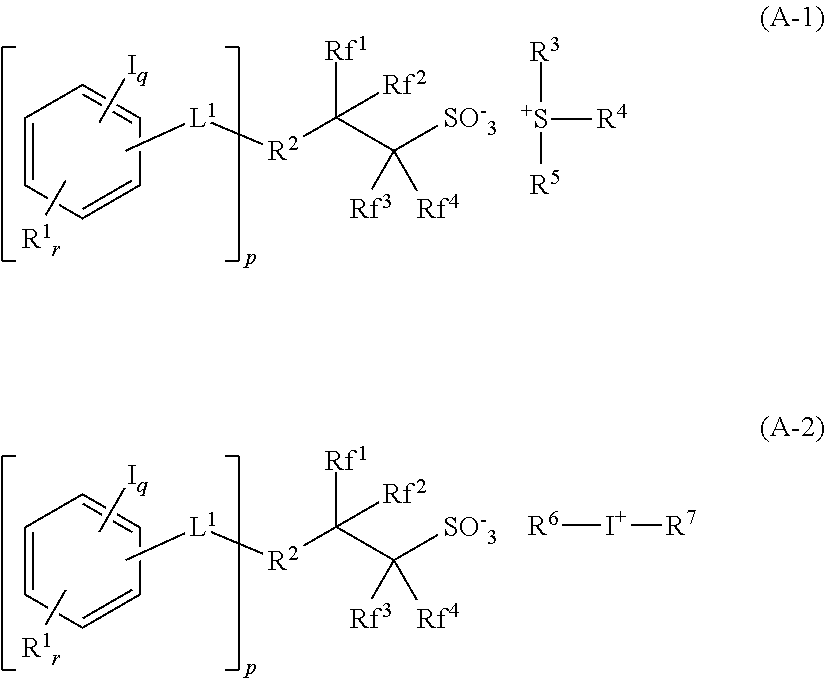
[0161]Acid generators, designated PAG 1 to PAG 21, used in resist compositions are identified below. PAG 1 to PAG 21 were synthesized by ion exchange between an ammonium salt of an iodized benzene ring-containing fluorosulfonic acid providing the anion shown below and a sulfonium or iodonium chloride providing the cation shown below.
[0162]
synthesis example
Synthesis of Base Polymers (Polymers 1 to 9, Comparative Polymers 1, 2)
[0163]Base polymers were prepared by combining suitable monomers, effecting copolymerization reaction thereof in tetrahydrofuran (THF) solvent, pouring the reaction solution into methanol for crystallization, repeatedly washing with hexane, isolation, and drying. The resulting polymers, designated Polymers 1 to 9 and Comparative Polymers 1 and 2, were analyzed for composition by 1H-NMR spectroscopy, and for Mw and Mw / Mn by GPC versus polystyrene standards using THF solvent.
[0164]
PUM
| Property | Measurement | Unit |
|---|---|---|
| of wavelength | aaaaa | aaaaa |
| wavelength | aaaaa | aaaaa |
| reaction temperature | aaaaa | aaaaa |
Abstract
Description
Claims
Application Information