Method for processing semiconductors using a combination of electron beam and optical lithography

a technology of electron beam and optical lithography, applied in the field of semiconductor processing, can solve the problems of multiple layers, poor optical alignment quality, and early use of metal layers, and achieve the effect of good optical alignment signal and superior alignment signal quality

Active Publication Date: 2014-06-17
RAYTHEON CO
View PDF26 Cites 3 Cited by
  • Summary
  • Abstract
  • Description
  • Claims
  • Application Information

AI Technical Summary

Benefits of technology

[0006]Thus, prior methods of mixing and matching optical and e-beam lithography systems developed for compound semiconductors have been based on alignment marks for the electron lithography system which are generated with the ohmic metal layer. This layer is itself aligned to an earlier layer having registration errors with respect to the initial optical alignment features imparted by the optical lithography step. Typically gold is a preferred metal layer for the electron beam alignment features because it's high atomic weight.
[0021]With such method, simultaneous patterning of optical alignment features and secondary or backscattered electron alignment features is achieved using a refractory metal nitride having both sufficient atomic weight and thickness to provide a strong backscattered or secondary alignment signal, and sufficient thickness to create a good optical alignment signal. Edge quality and is improved over gold features having larger grain size, and the refractory metal nitride is unaffected by subsequent high temperature operations.
[0022]The use a refractory metal or a refractory metal compound of sufficient atomic weight allows optimization of a dedicated alignment layer for optical alignment signal quality while simultaneously optimizing the layer for backscattered and secondary electron alignment signal quality. Specifically the use of a tantalum nitride (TaN) film was shown to exhibit superior alignment signal quality in both optical and e-beam alignment systems and remain stable when subjected to a high temperature ohmic alloy process step.

Problems solved by technology

The inventors have recognized that for some semiconductor devices, early use of metal layers can pose a contamination risk during subsequent high temperature operations.
More particularly, while with GaAs device fabrication the ohmic metal provides an adequate alignment signal due to differences in the metals composition and alloy conditions; the inventors have recognized that the alloy conditions and composition of the ohmic metal for GaN is different than the ohmic metal on GaAs and that with GaN the alloyed ohmic metal edges are very rough thereby making its use as an alignment mark for subsequent electron beam alignment undesirable nature of the post alloyed ohmic metal.
The ohmic contact metal is also used to provide alignment marks for subsequent electron beam lithography to be used in forming the gate contacts; however, they may not be adequate in providing accurate alignment to the mesas alignment mark.
More particularly, ohmic metal has been used for optical alignment as well as electron beam alignment, but the issue remains that you now have multiple layers which are aligned to different features.
The alignment marks defined in an ohmic contact are often not the optimum thickness or surface roughness for alignment purposes.
As noted above, the inventors have recognized that with a GaN process the ohmic alignment marks are so rough that they are not useful for e-beam alignment, and another metal layer has had to be added to define the e-beam alignment marks.

Method used


Image

  • Method for processing semiconductors using a combination of electron beam and optical lithography
  • Method for processing semiconductors using a combination of electron beam and optical lithography
  • Method for processing semiconductors using a combination of electron beam and optical lithography

Examples


Embodiment Construction

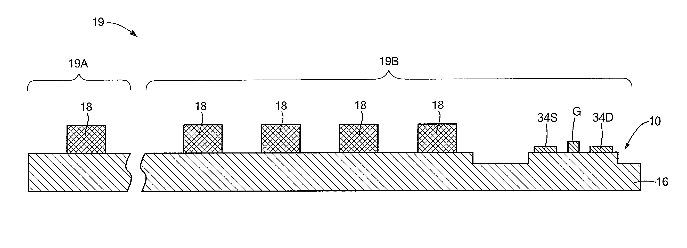
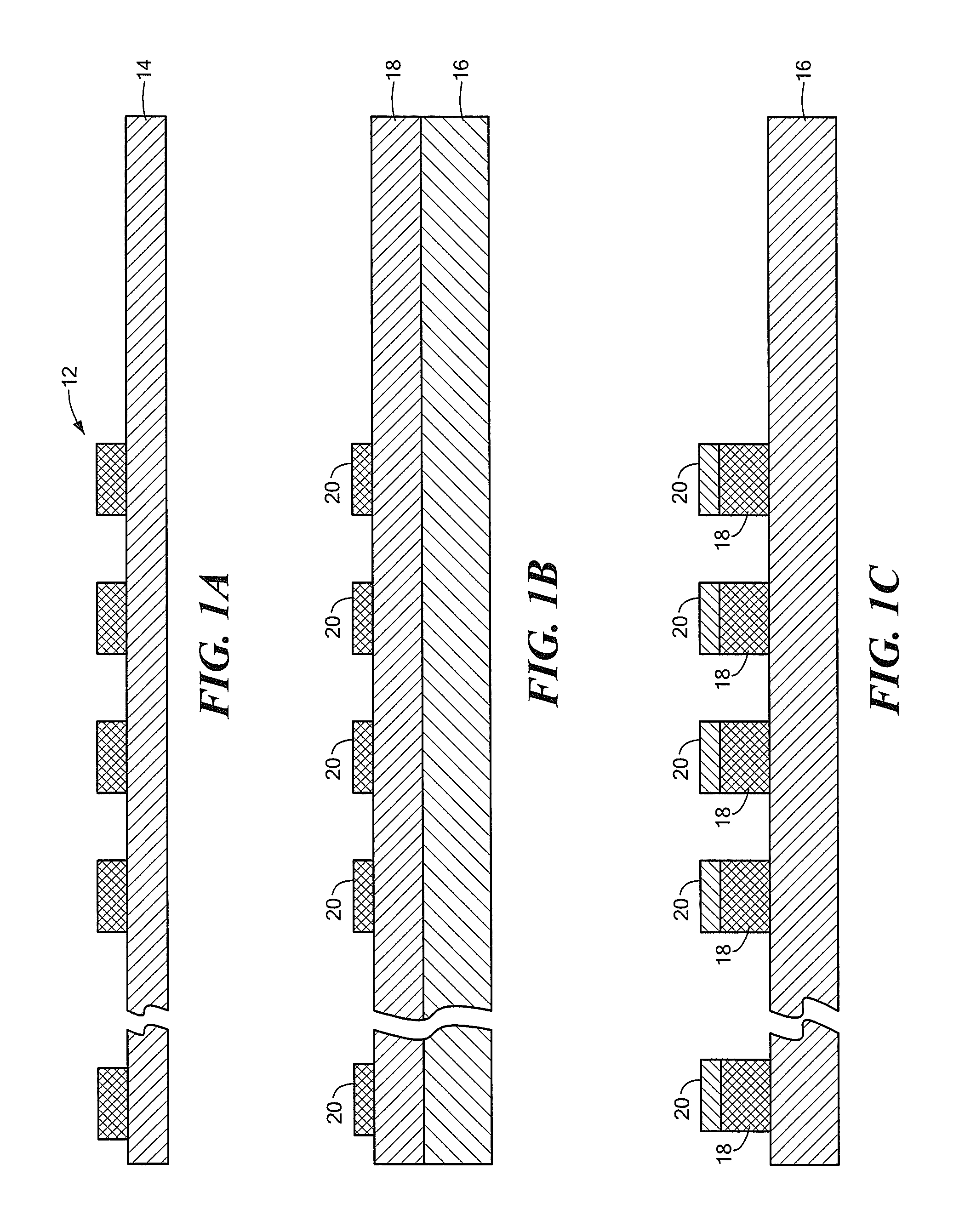
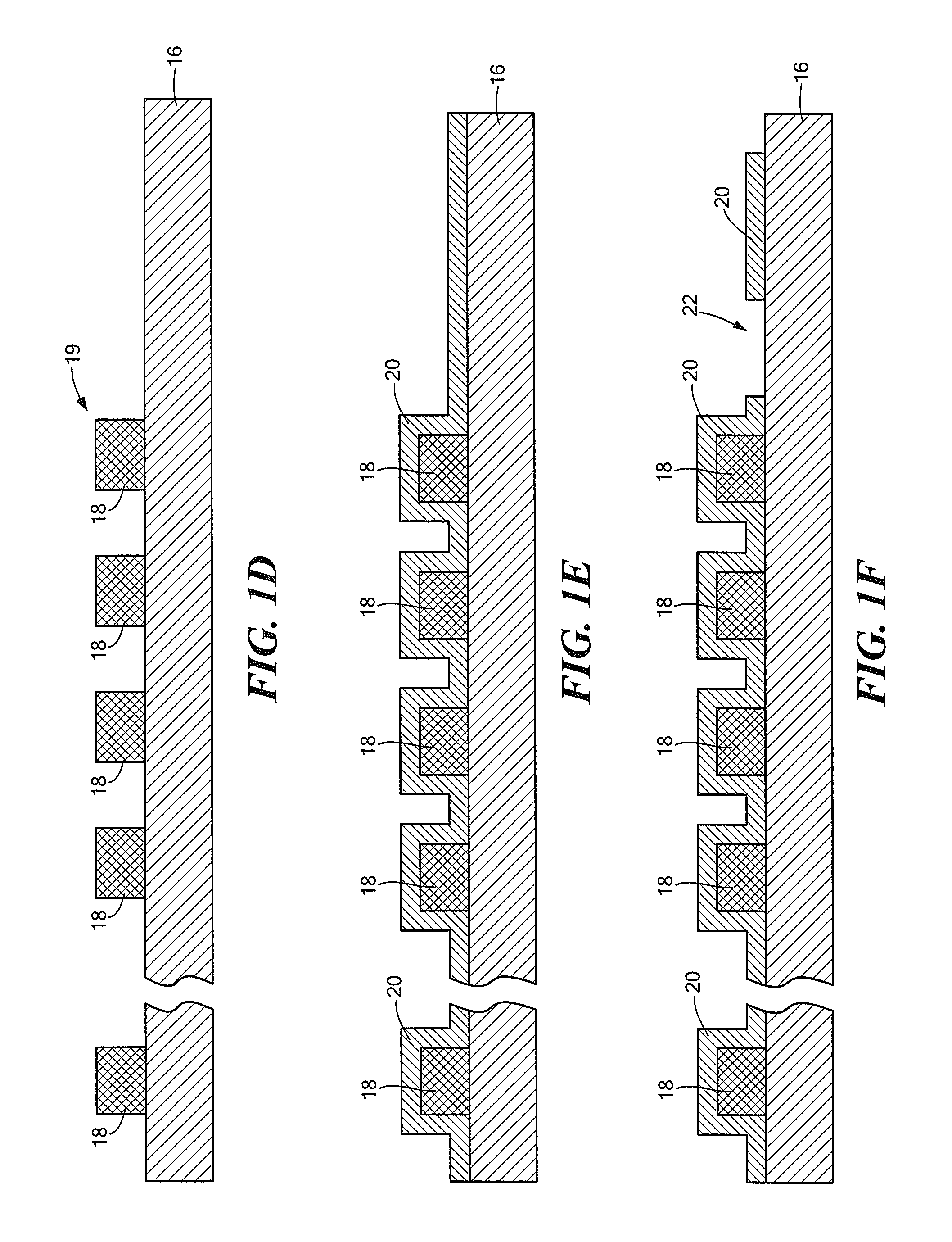
[0032]Referring now to FIGS. 1A through 1P, a process for foaming a semiconductor device, here a Field Effect Transistor (FET) 10 (FIG. 1P) is shown. First, an alignment mark pattern 12 is formed on an optical lithographic reticle 14 (FIG. 1A). The pattern 12 has two portions: an electron beam alignment pattern portion 12a and an optical alignment pattern portion 12b. A semiconductor substrate 16, here GaN, having a layer 18 of metal deposited on the upper surface of the substrate 16 (i.e., the zero layer of the process) is coated with a layer of photoresist material 20 (FIG. 1B). The metal material in layer 18 is a refractory metal or a refractory metal compound, here for example TaN having a thickness of 500 Angstroms. Other materials may be used for metal layer 18, for example, Hafnium, Tantalum, Tungsten, Rhenium, or compounds thereof such as when combined with nitrogen, or metals having an atomic weight greater than 60.

[0033]Next, the alignment mark pattern 12 on the reticle 14...


PUM


Abstract

Forming an alignment mark on a semiconductor structure using an optical lithography to form a metal alignment mark on a substrate of the structure, using the formed metal alignment mark to form a first feature of a semiconductor device being formed on the substrate using optical lithography, and using the formed metal alignment mark to form a second, different feature for the semiconductor using electron beam lithography. In one embodiment, the first feature is an ohmic contact, the second feature is a Schottky contact, the metal alignment mark is a refractory metal or a refractory metal compound having an atomic weight greater than 60 such as TaN and the semiconductor device is a GaN semiconductor device. A semiconductor structure having a metal alignment mark on a zero layer of the structure, the metal alignment mark is a TaN and the semiconductor is GaN.

Description

TECHNICAL FIELD[0001]This disclosure relates generally to methods for processing semiconductors and more particularly to methods for processing semiconductors using a combination of electron beam and optical lithography.BACKGROUND AND SUMMARY[0002]As is known in the art, fabrication of semiconductor devices utilizing a combination of electron beam (i.e., e-beam) and optical lithography systems requires alignment features that are optimized for both systems and are placed on the substrate with minimum placement errors between the two sets of features. More particularly, optical lithography uses alignment marks etched into a semiconductor substrate while electron beam lithography requires metal alignment marks. Further, there is less backscatter of electrons from the semiconductor than from metal. Further, while electron beam lithography is slower than optical lithography, electron beam lithography is able to produce smaller features than optical lithography. Another requirement for t...

Claims


Application Information

Patent Timeline
Patent Type & Authority Patents(United States)
IPC IPC(8): H01L21/30H01L29/201
CPCG03F9/7076H01L23/544H01L2223/54453G03F9/708H01L2223/54426H01L2223/5442H01L21/71H01L2924/0002H01L2924/00
Inventor DUVAL, PAUL J.TABATABAIE, KAMALDAVIS, WILLIAM J.
Owner RAYTHEON CO
Why Eureka
Try Eureka