Ceramic electrostatic chuck having a V-shape seal band

a technology of electrostatic chuck and seal band, which is applied in the direction of semiconductor/solid-state device manufacturing, basic electric elements, electric devices, etc., can solve the problems of electrostatic chuck bonding problems, contamination in the chamber, and only providing marginal protection

Active Publication Date: 2021-03-09
APPLIED MATERIALS INC
View PDF18 Cites 0 Cited by
  • Summary
  • Abstract
  • Description
  • Claims
  • Application Information

AI Technical Summary

Benefits of technology

[0003]To drive down manufacturing cost, integrated chip (IC) manufactures demand higher throughput and better device yield and performance from every silicon substrate processed. Conventional electrostatic chucks (ESC) are typically bonded to a cooling plate in a substrate support assembly. The bond may be protected with a seal. However, the seals only provide a marginal protection due to a minimal surface contact between the ESC and the cooling plate. The electrostatic chuck may experience bonding problems within the substrate support assemblies due to fluorine radical penetration etching away the bonding layer once the seal has been compromised. Loss of bond material accelerates delamination of the ESC from the cooling plate. Additionally, a compromised seal may cause the bond material to outgas into the processing volume, thereby causing contamination in the chamber. The chamber may require down time to repair or replace the substrate support assembly, effecting costs, yield and performance.

Problems solved by technology

Reliably producing nanometer and smaller features is one of the key technology challenges for next generation very large scale integration (VLSI) and ultra large-scale integration (ULSI) of semiconductor devices.
However, as the limits of circuit technology are pushed, the shrinking dimensions of VLSI and ULSI interconnect technology have placed additional demands on processing capabilities.
However, the seals only provide a marginal protection due to a minimal surface contact between the ESC and the cooling plate.
The electrostatic chuck may experience bonding problems within the substrate support assemblies due to fluorine radical penetration etching away the bonding layer once the seal has been compromised.
Additionally, a compromised seal may cause the bond material to outgas into the processing volume, thereby causing contamination in the chamber.
The chamber may require down time to repair or replace the substrate support assembly, effecting costs, yield and performance.

Method used


Image

  • Ceramic electrostatic chuck having a V-shape seal band
  • Ceramic electrostatic chuck having a V-shape seal band
  • Ceramic electrostatic chuck having a V-shape seal band

Examples


Embodiment Construction

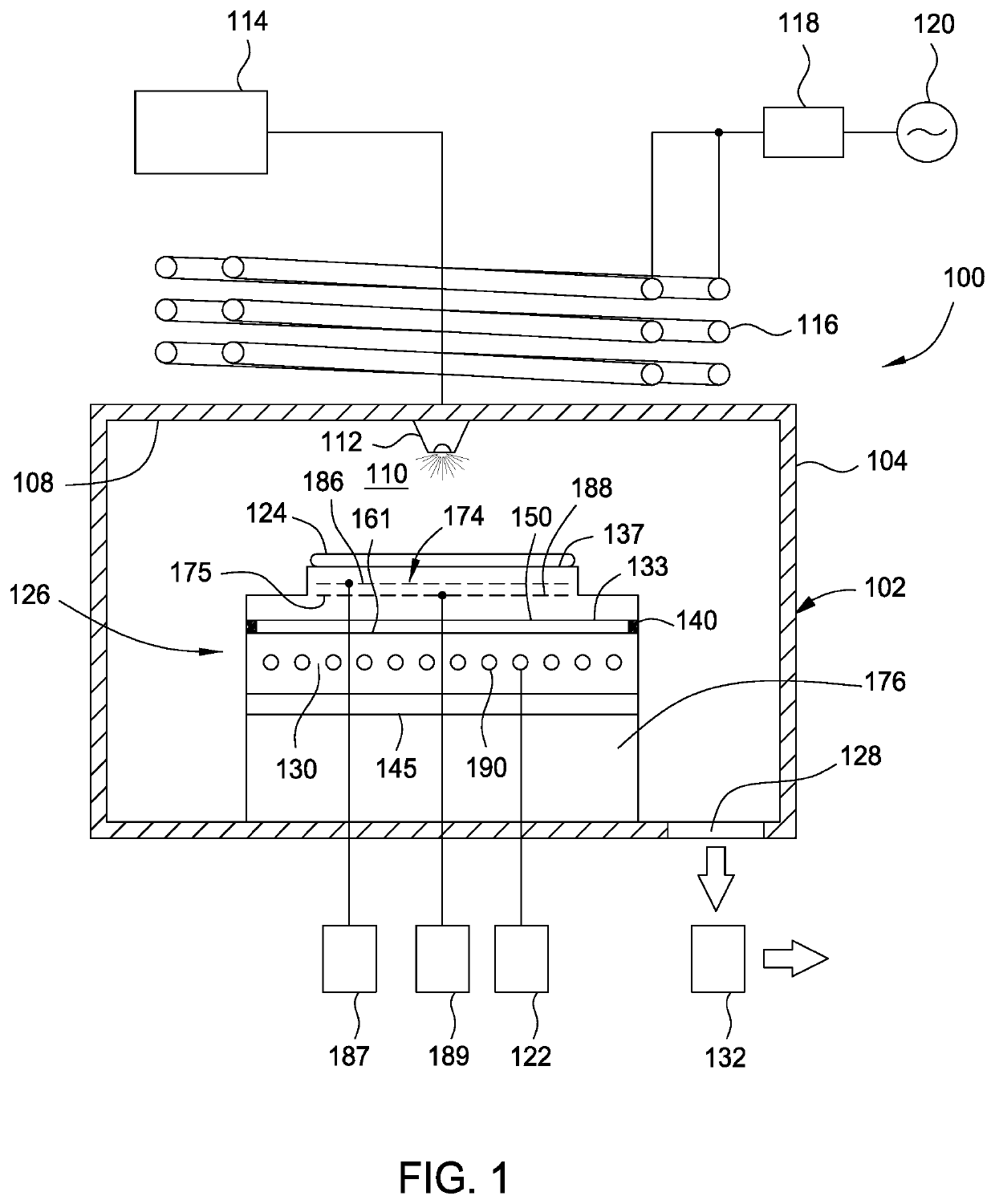
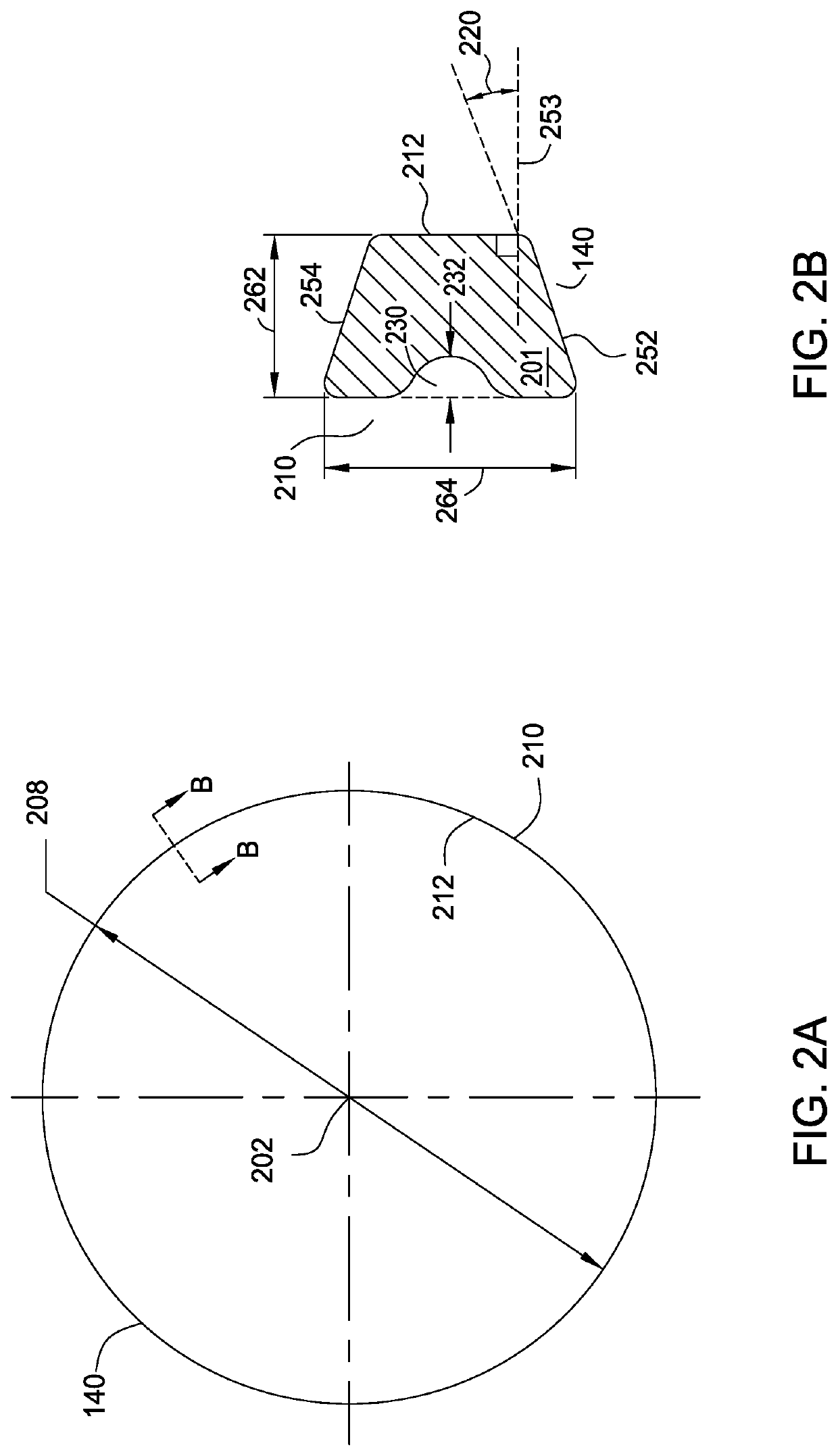
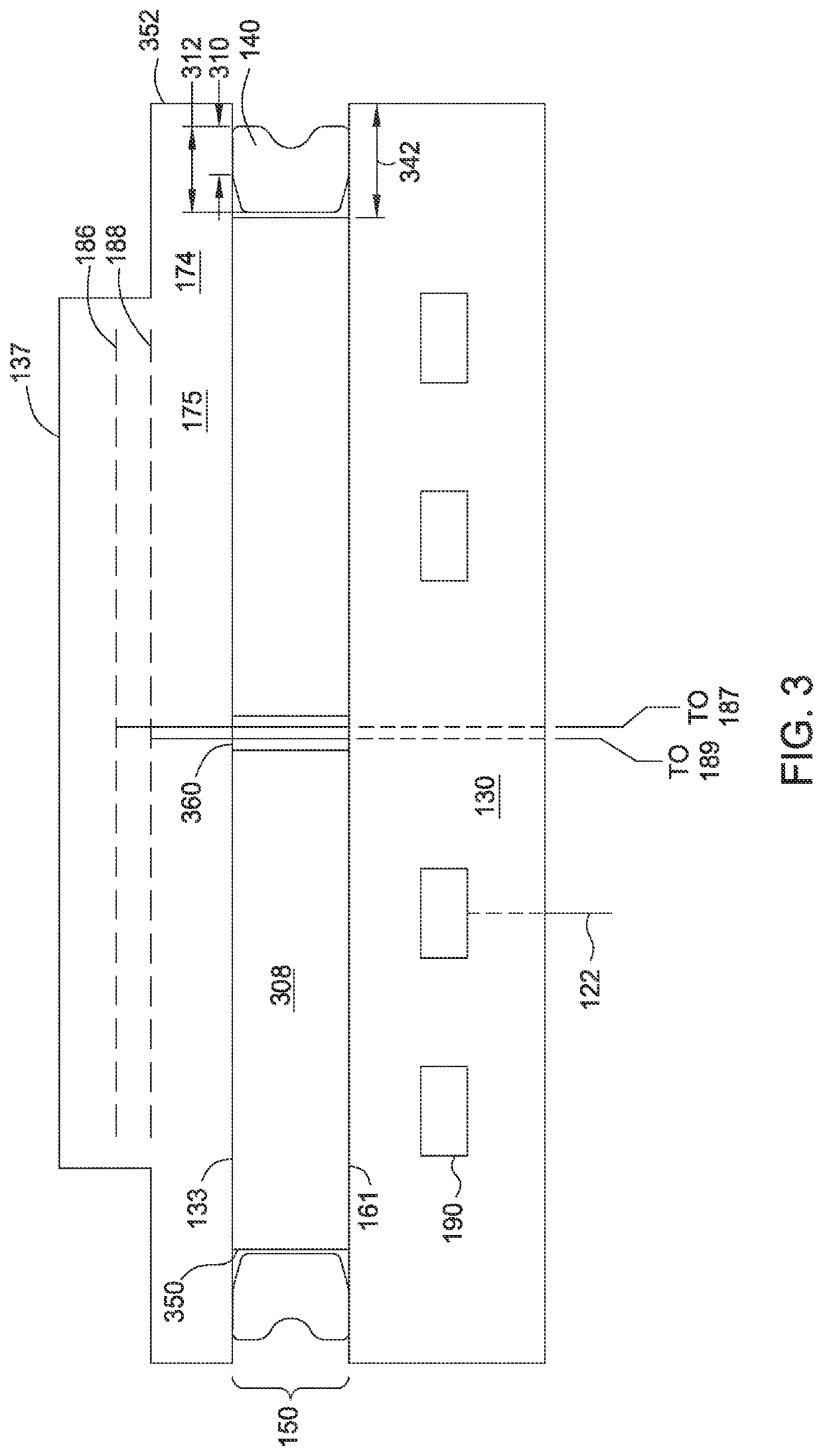
[0012]Implementations described herein provide a substrate support assembly that includes a seal band. The seal band protects an adhesive layer that is disposed between an electrostatic chuck (ESC) and a cooling plate of the substrate support assembly. The seal band is particularly advantageous for ESC applications that are exposed to high temperature operation. High temperature is intended to refer to temperatures in excess of about 150 degrees Celsius, for example, temperatures in excess of about 250 degrees Celsius, such as temperatures of about 250 degrees Celsius to about 300 degrees Celsius. The seal band is disposed on the outer perimeter of the bonding layer to prevent the bonding material from outgassing or being attacked by the harsh chamber environment. The seal band is configured to have increased contact area for maintaining the integrity and longevity of the seal. Although the substrate support assembly is described below in an etch processing chamber, the substrate su...


PUM


Abstract

Implementations described herein provide a substrate support assembly that includes a seal band. The seal band protects an adhesive layer that is disposed between an electrostatic chuck (ESC) and a cooling plate of the substrate support assembly. In one example, a substrate support assembly includes an electrostatic chuck and a cooling plate. A bonding layer secures a bottom surface of the electrostatic chuck to a top surface of the cooling plate. The bonding layer has an adhesive layer and a seal band. The seal band circumscribes and protects the adhesive layer. The seal band has a ring shaped body. The ring shaped body has a top surface connected to a bottom surface by an inner surface and an outer surface. The top surface and the bottom surface angled less than 85 degrees from the inner surface. The outer surface has an indent formed therein.

Description

BACKGROUNDField[0001]Implementations described herein generally relate to semiconductor manufacturing and more particularly to a substrate support assembly suitable for high temperature semiconductor manufacturing.Description of the Related Art[0002]Reliably producing nanometer and smaller features is one of the key technology challenges for next generation very large scale integration (VLSI) and ultra large-scale integration (ULSI) of semiconductor devices. However, as the limits of circuit technology are pushed, the shrinking dimensions of VLSI and ULSI interconnect technology have placed additional demands on processing capabilities. Reliable formation of gate structures on the substrate is important to VLSI and ULSI success and to the continued effort to increase circuit density and quality of individual substrates and die.[0003]To drive down manufacturing cost, integrated chip (IC) manufactures demand higher throughput and better device yield and performance from every silicon ...

Claims


Application Information

Patent Timeline
Patent Type & Authority Patents(United States)
IPC IPC(8): H01L21/67H01L21/683H01L21/687
CPCH01L21/6833H01L21/67109H01L21/67126H01L21/6831H01L21/68785H01L21/67103F16J15/022
Inventor NOORBAKHSH, HAMIDNAKAGAWA, IPPEIYOSHIDA, NOBUHIRO
Owner APPLIED MATERIALS INC
Why Eureka
Try Eureka