Display panel and display device

a display panel and display device technology, applied in the field of display, can solve problems such as unstable excited state in normal environment, and achieve the effects of improving productivity and yield, reducing process flow, and improving light transmittance at the groov

Active Publication Date: 2021-10-19
WUHAN CHINA STAR OPTOELECTRONICS SEMICON DISPLAY TECH CO LTD
View PDF16 Cites 0 Cited by
  • Summary
  • Abstract
  • Description
  • Claims
  • Application Information

AI Technical Summary

Benefits of technology

[0017]The present invention relates to the display panel and the display device. On the one hand, the groove forms on one side of the packaging layer of the display area away from the substrate, and extends downward to one side of the antireflective film facing the thin film transistor layer; and the camera is disposed on one side of the substrate away from the thin film transistor layer and is corresponding the groove, thereby reducing process flow, improving productivity and yield, and realizing the full screen. On the other hand, the present invention also adds the antireflective film to improve the light transmittance at the groove and avoid the phenomenon that the camera is difficult to image.

Problems solved by technology

But the excited state is unstable in normal environment.

Method used


Image

  • Display panel and display device
  • Display panel and display device

Examples


embodiment 1

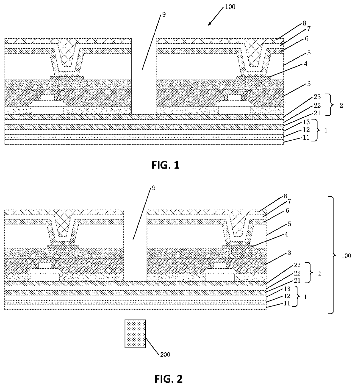
[0028]Referring to FIG. 1, a display panel 100 defines a display area, and includes a substrate 1, an antireflective film 2, a thin film transistor layer 3, anodes 4, a pixel definition layer 5, a light emitting layer 6, a cathode 7 and a packaging layer 8.

[0029]Wherein, the substrate 1 includes a first underlayer 11, an intermediate layer 12 and a second underlayer 13. The thicknesses of the first underlayer 11 and the second underlayer 13 are 6-10 microns (μm). If the thicknesses of the first underlayer 11 and the second underlayer 13 are less than 6 μm, the production cost thereof will increase due to production process problems. If the thicknesses of the first underlayer 11 and the second underlayer 13 are greater than 10 μm, the overall thickness of the display panel 100 will increase, which affects the beauty of the product and the feel of the use. The material of the first underlayer 11 and the second underlayer 13 can be polyimide, and the first underlayer 11 and the second ...

embodiment 2

[0035]The differences between the second embodiment and the first embodiment are explained below, and their similarities are not repeated here.

[0036]Referring to FIG. 2, the embodiment further provides a display device, which includes the display panel 100 of the present invention and a camera 200 located under the display panel 100. The camera 200 is located under the display panel 100 and is corresponding to the groove 9. Thus, the display area can be increased and the full screen can be achieved.

[0037]Specifically, a projection area of the groove 9 in the display panel 100 can be larger than that of the camera 200, so as to increase a lighting area of the camera 200, improve an imaging effect of the camera 200 and increase a customer experience.

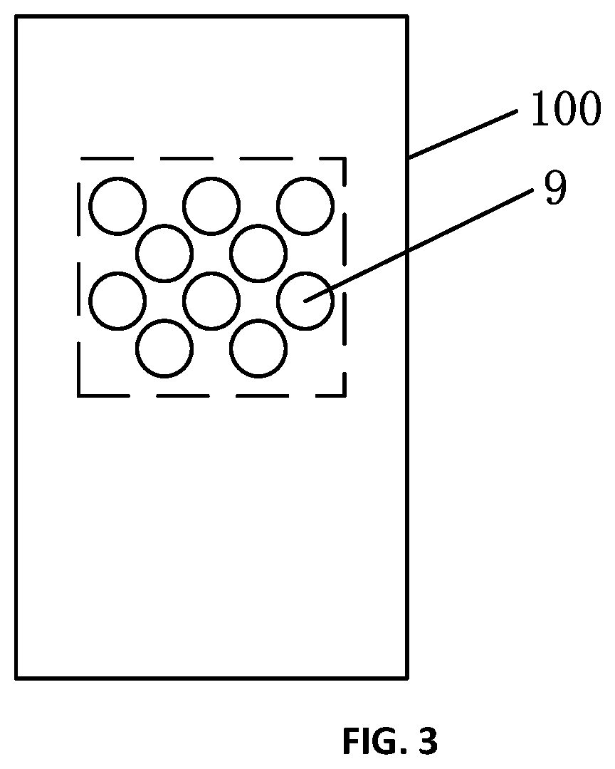
[0038]As shown in FIG. 3, in the actual production, the number of the groove 9 can be increased to two or more. The grooves 9 are arranged to form an open area shown by dotted lines in the drawing. The camera 200 is corresponding to the op...


PUM

PropertyMeasurementUnit
thicknessesaaaaaaaaaa
thicknessaaaaaaaaaa
thicknessaaaaaaaaaa

Abstract

The present invention relates to a display panel and a display device. On the one hand, the display panel disposes a groove, which forms on one side of a packaging layer of a display area away from a substrate, and extends downward to one side of an antireflective film facing a thin film transistor layer; and a camera is disposed on one side of the substrate away from the thin film transistor layer and is corresponding the groove, thereby reducing process flow, improving productivity and yield, and realizing a full screen. On the other hand, the present invention also adds an antireflective film to improve the light transmittance at the groove and avoid the phenomenon that the camera is difficult to image.

Description

BACKGROUND OF THE INVENTION1. Field of the Invention[0001]The present disclosure relates to a display technical field, and more particularly to a display panel and a display device.2. Description of the Prior Art[0002]An OLED (Organic Light-Emitting Diode) device is also called an organic electro-laser display device and an organic light-emitting semiconductor. The basic structure of the OLED is a sandwich-like structure constructed by a thin transparent indium tin oxide (ITO) with semiconductor properties connected to an anode of a power and a metal surface cathode. The whole structure includes a hole transport layer (HTL), an electroluminescent layer (EL) and an electron transport layer (ETL). When the power is supplied to an appropriate voltage, holes of the anode and electrons of the surface cathode will combine in the electroluminescent layer, and form excitons (electron-hole pairs) in an excited state with a certain probability under the action of a Coulomb force. But the exci...

Claims


Application Information

Patent Timeline
Patent Type & Authority Patents(United States)
IPC IPC(8): H01L51/52H01L27/32
CPCH01L51/5253H01L27/3234H01L27/3246H10K59/65H10K59/12H10K50/84H10K50/85H04M1/0266H04M1/0264H10K59/124H10K59/122H10K50/86H10K50/844
Inventor ZHENG, YING
Owner WUHAN CHINA STAR OPTOELECTRONICS SEMICON DISPLAY TECH CO LTD
Why Eureka
Try Eureka