Leadframe substrate having modulator and crack inhibiting structure and flip chip assembly using the same
a technology of modulator and substrate, which is applied in the manufacture of printed circuits, printed circuit aspects, basic electric elements, etc., can solve the problems of imposing thermal stress on the chip, prone to cracking of contact areas between heat dissipation elements b>12/b> and adhesive b>17/b>, and avoiding the cracking of the interconnection bump associated with chip/substrat cte-mismatch, and avoiding damage to top routing tra
- Summary
- Abstract
- Description
- Claims
- Application Information
AI Technical Summary
Benefits of technology
Problems solved by technology
Method used
Image

Examples
embodiment 1
[0052]FIGS. 2-11 are schematic views showing a method of making an untrimmed leadframe substrate that includes a metal frame, a plurality of metal leads, a modulator, a resin layer, a first crack inhibiting structure and a first routing trace in accordance with the first embodiment of the present invention.
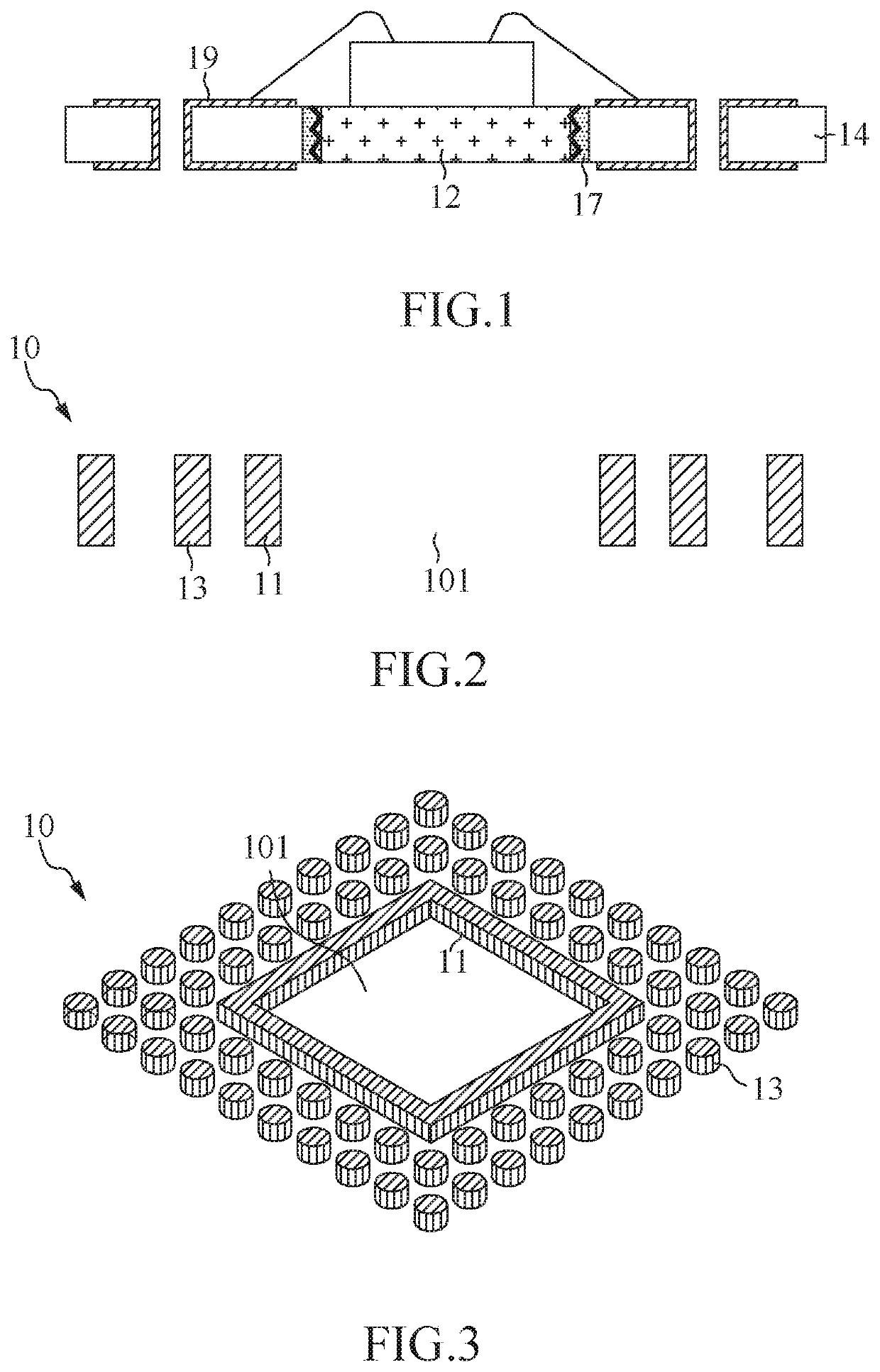
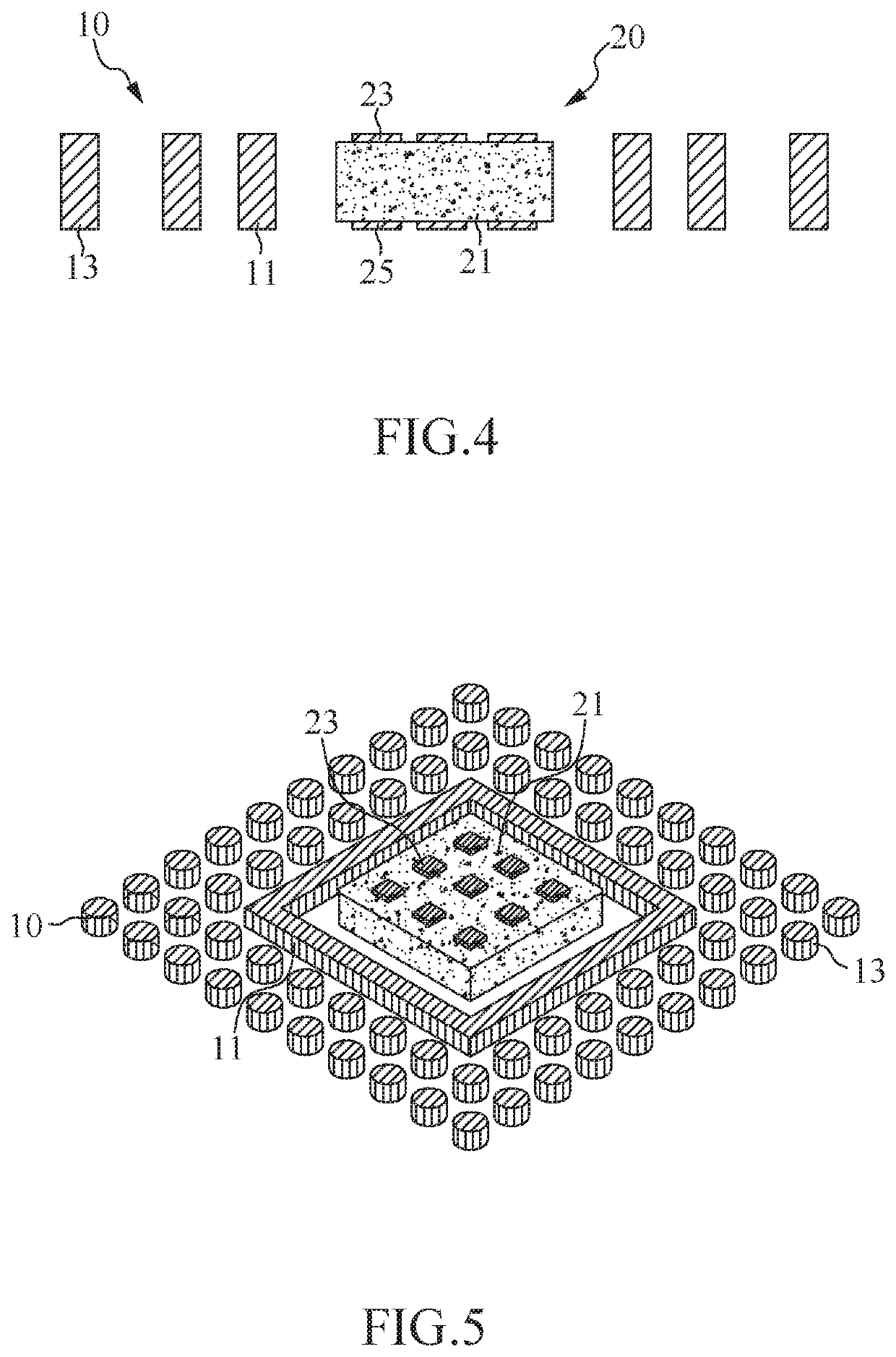
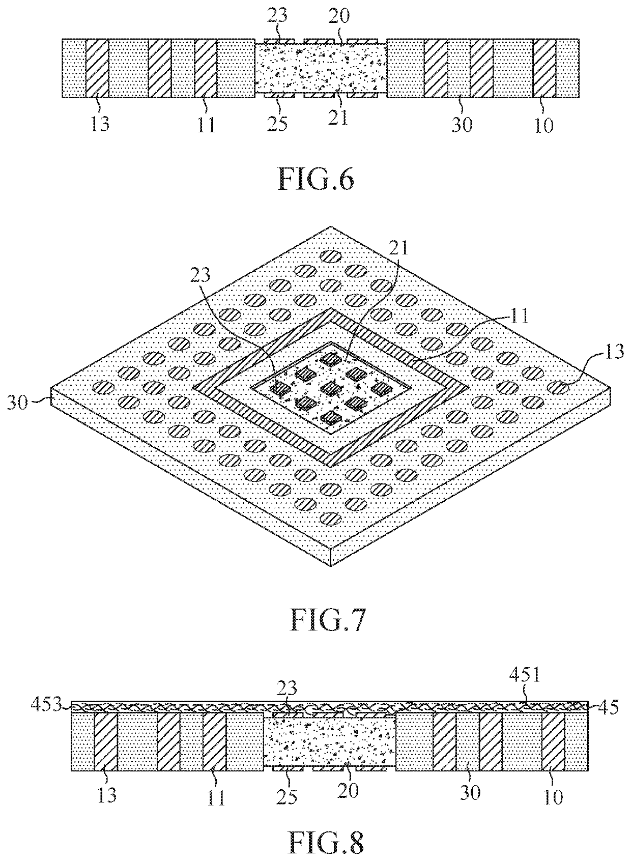
[0053]FIGS. 2 and 3 are cross-sectional and top perspective views, respectively, of a leadframe 10. The leadframe 10 typically is made of copper alloys, steel or alloy 42, and can be formed by wet etching or stamping / punching process from a rolled metal strip. The etching process may be a one-sided or two-sided etching to etch through the metal strip and thereby transfers the metal strip into a desired overall pattern of the leadframe 10. In this embodiment, the leadframe 10 has a uniform thickness in a range from about 0.15 mm to about 1.0 mm, and includes a metal frame 11 and a plurality of metal leads 13. The metal frame 11 has planar top and bottom surfaces and an aperture 101...
embodiment 2
[0065]FIG. 17 is a cross-sectional view of a leadframe substrate in accordance with the second embodiment of the present invention.
[0066]For purposes of brevity, any description in Embodiment 1 is incorporated herein insofar as the same is applicable, and the same description need not be repeated.
[0067]The leadframe substrate 200 is similar to that illustrated in FIG. 10, except that it further includes a second crack inhibiting structure 55 and a second routing trace 56 formed in an alternate fashion from below. The second crack inhibiting structure 55 covers the bottom surface of the metal frame 11, the bottom ends of the metal leads 13, the bottom side of the modulator 20, and the bottom surface of the resin layer 30 to provide protection from below. The second routing trace 56 extends laterally on the second crack inhibiting structure 55, and is thermally conductible to the bottom contact pads 25 of the modulator 20 as well as the metal frame 11 and electrically connected to the...
embodiment 3
[0072]FIG. 21 is a cross-sectional view of a leadframe substrate in accordance with the third embodiment of the present invention.
[0073]For purposes of brevity, any description in Embodiments above is incorporated herein insofar as the same is applicable, and the same description need not be repeated.
[0074]The leadframe substrate 300 is similar to that illustrated in FIG. 10, except that the modulator 20 further has metal through vias 27 in contact with the top contact pads 23 and the bottom contact pads 25. The metal through vias 27 extend through the thermally conductive and electrically insulating slug 21 to provide electrical connection between the top contact pads 23 and the bottom contact pads 25 for ground / power connection.
[0075]FIG. 22 is a cross-sectional view of a semiconductor assembly 310 with a semiconductor chip 61 electrically connected to the leadframe substrate 300 illustrated in FIG. 21. The semiconductor chip 61 is face-down mounted to the first routing trace 46 t...
PUM
| Property | Measurement | Unit |
|---|---|---|
| elastic modulus | aaaaa | aaaaa |
| thickness | aaaaa | aaaaa |
| diameter | aaaaa | aaaaa |
Abstract
Description
Claims
Application Information
 - R&D
- Intellectual Property
- Life Sciences
- Materials
- Tech Scout
- Unparalleled Data Quality
- Higher Quality Content
- 60% Fewer Hallucinations
Browse by: Latest US Patents, China's latest patents, Technical Efficacy Thesaurus, Application Domain, Technology Topic, Popular Technical Reports.
© 2025 PatSnap. All rights reserved.Legal|Privacy policy|Modern Slavery Act Transparency Statement|Sitemap|About US| Contact US: help@patsnap.com