Method for fastening a semiconductor chip on a substrate, and electronic component

a technology of semiconductor chips and electronic components, applied in semiconductor devices, semiconductor/solid-state device details, electrical devices, etc., can solve the problems of initiation of cracks, significant thermally induced mechanical loads, carrier materials, etc., and achieve the effects of less brittleness, less brittleness, and more resilient mechanical properties

Active Publication Date: 2022-04-26
OSRAM OLED
View PDF22 Cites 1 Cited by
  • Summary
  • Abstract
  • Description
  • Claims
  • Application Information

AI Technical Summary

Benefits of technology

[0021]According to at least one embodiment, the indium-tin alloy of the second metallic layer has the formula InxSn1-x with 0.04≤x≤0.2, preferably 0.06≤x≤0.18, particularly preferably 0.08≤x≤0.16. The second metallic layer preferably consists of the indium-tin alloy of the formula InxSn1-x with 0.04≤x≤0.2. Such a composition of the indium-tin alloy has proven to be particularly advantageous. Due to the low indium content, the melting point decreases in comparison to pure tin, as a result of which the temperature in method step F) can be kept low. In addition, it can be ensured with a maximum indium content of x=0.2 that the indium-tin alloy does not melt before the semiconductor chip is applied to the substrate in optional further method steps. Surprisingly, it has also been shown that the wetting properties of the metallization layer sequence are best when the indium content does not exceed x=0.2.
[0067]According to at least one embodiment, the third intermetallic layer comprises at least one gold-tin alloy of the formula Au1-ySny with 0.10≤y≤0.185. A gold-tin alloy of the zeta phase is particularly preferentially formed. In addition to the gold-tin alloy of the formula Au1-ySnywith 0.10≤y≤0.185 or the gold-tin alloy of the zeta phase, further gold-tin alloys and / or gold-tin-indium alloys can be comprised in the third intermetallic layer. A gold-tin alloy of the formula Au1-ySny with 0.10≤y≤0.185 or a gold-tin alloy of the zeta phase is particularly preferred as the main component of the third intermetallic layer. Such a third intermetallic layer has proven to be particularly advantageous in terms of its mechanical properties and is in particular more resilient, ductile and significantly less brittle than a gold-tin alloy with a higher tin content or a lower gold content. This makes the electronic component particularly stable against mechanical loads.

Problems solved by technology

Due to the difference in the thermal expansion behavior between the semiconductor chip and the material of the substrate, tensions arise during cooling from the soldering temperature to room temperature in the composite of semiconductor chip and substrate.
These can lead to the initiation of cracks, for example, in the carrier material of the semiconductor chip, if the electronic component is subjected to mechanical load.
With this solder the soldering temperature is in the range of 300° C. Due to the high soldering temperature and the different thermal expansion behavior, considerable thermally induced mechanical loads occur during the cooling of the composite of substrate and semiconductor chip.
If the component is subjected to further mechanical load, this can lead to failure of the solder joint or to the initiation of cracks in the substrate or the solder joint.

Method used


Image

  • Method for fastening a semiconductor chip on a substrate, and electronic component
  • Method for fastening a semiconductor chip on a substrate, and electronic component
  • Method for fastening a semiconductor chip on a substrate, and electronic component

Examples


Embodiment Construction

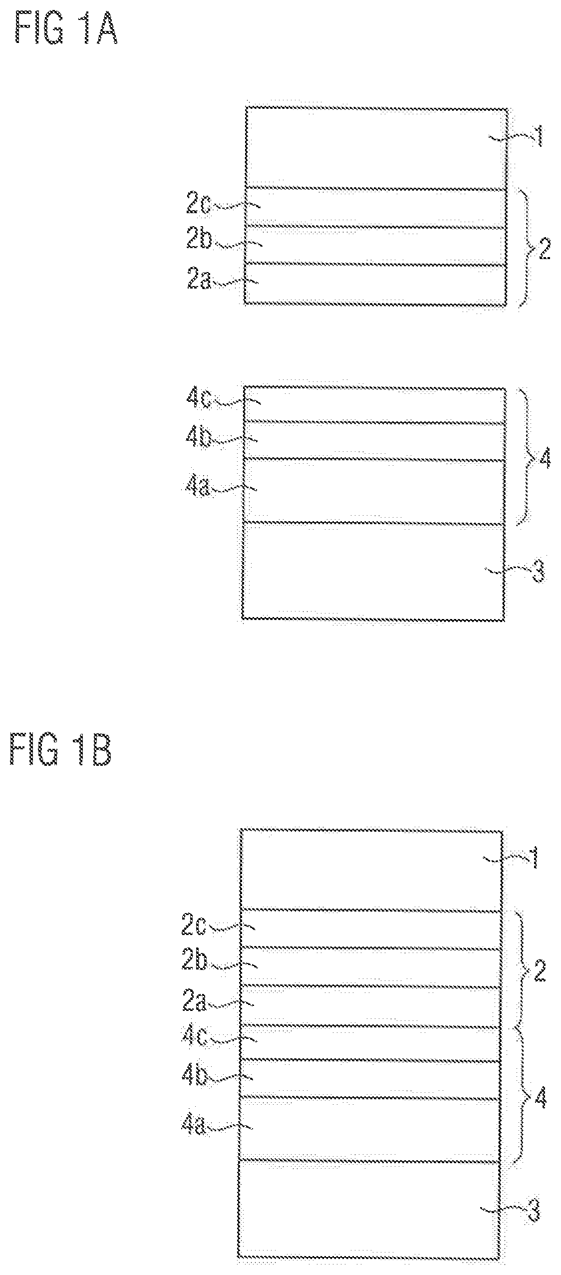
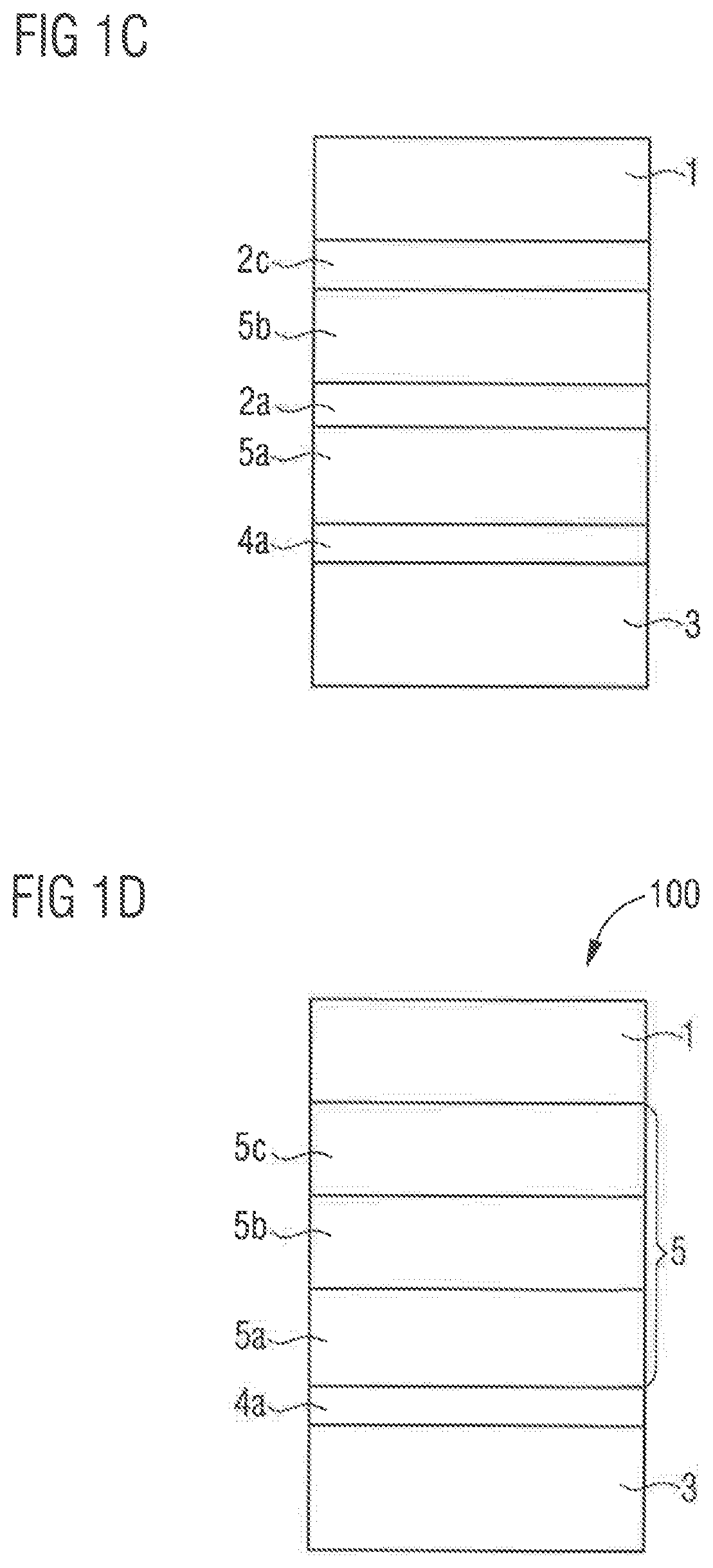
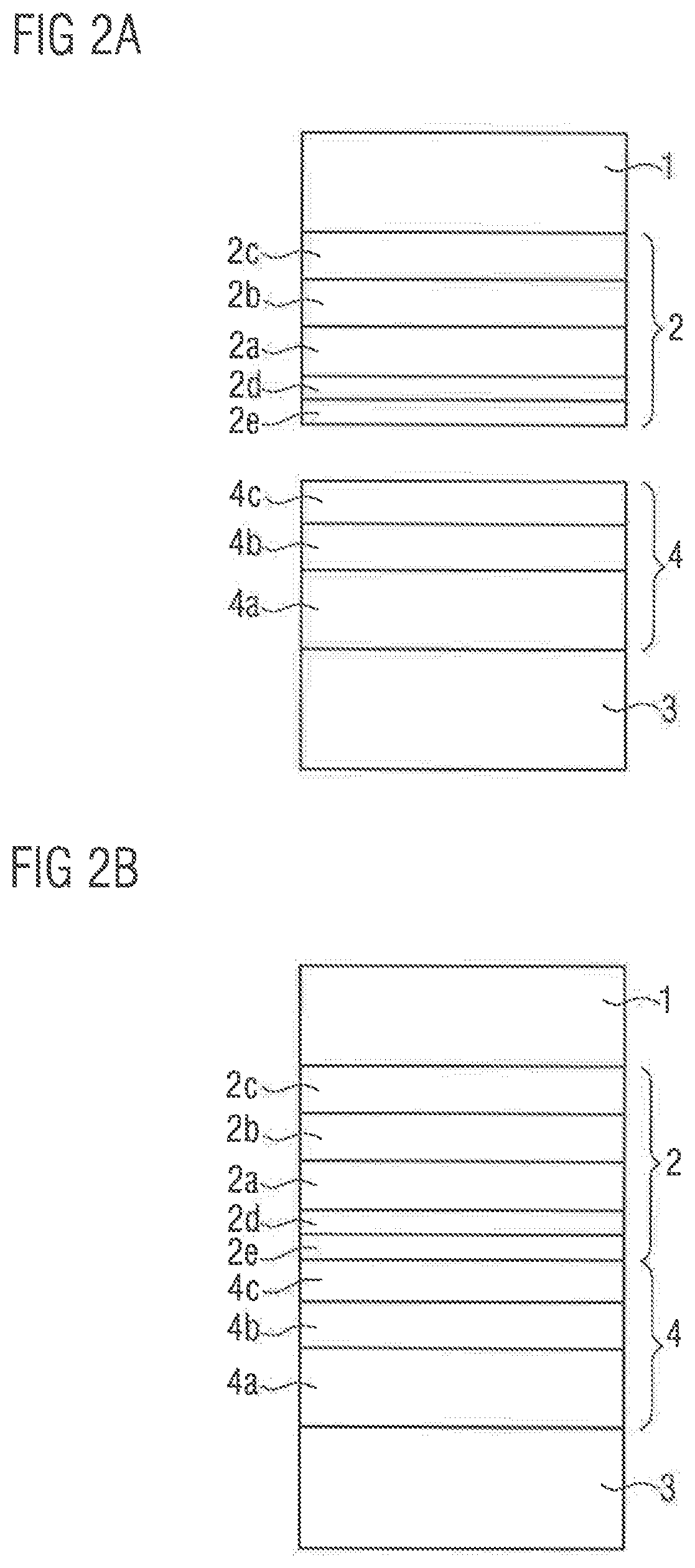
[0076]FIG. 1A shows a semiconductor chip 1 above which a solder metal layer sequence 2 is arranged. The solder metal layer sequence comprises a first metallic layer 2a, a barrier layer 2b arranged above the first metallic layer 2a and a second metallic layer 2c arranged above the barrier layer 2b. The first metallic layer 2a comprises or consists of an indium-tin alloy of the formula InxSn1-x with 0.04≤x≤0.2. The barrier layer 2b consists of nickel, titanium or platinum and the second metallic layer 2c consists of gold. The amount of substance of the gold of the second metallic layer 2c is greater than the amount of substance of the tin of the first metallic layer 2a. The first metallic layer 2a has a layer thickness between 750 nm and 3 μm inclusive, the barrier layer has a layer thickness between 5 nm and 200 nm inclusive and the second metallic layer 2c has a layer thickness between 500 nm and 2 μm inclusive. Further, FIG. 1A shows a substrate 3 above which a metallization layer ...


PUM

PropertyMeasurementUnit
thicknessaaaaaaaaaa
thicknessaaaaaaaaaa
thicknessaaaaaaaaaa

Abstract

A method for fastening a semiconductor chip on a substrate and an electronic component are disclosed. In an embodiment a method includes providing a semiconductor chip, applying a solder metal layer sequence on the semiconductor chip, providing a substrate, applying a metallization layer sequence on the substrate, applying the semiconductor chip on the substrate via the solder metal layer sequence and the metallization layer sequence and heating the applied semiconductor chip on the substrate for fastening the semiconductor chip on the substrate. The solder metal layer may include a first metallic layer comprising an indium-tin alloy, a barrier layer arranged above the first metallic layer and a second metallic layer comprising gold arranged between the barrier layer and the semiconductor chip, wherein an amount of substance of the gold in the second metallic layer is greater than an amount of substance of tin in the first metallic layer.

Description

[0001]This patent application is a national phase filing under section 371 of PCT / EP2018 / 064914, filed Jun. 6, 2018, which claims the priority of German patent application 102017112866.2, filed Jun. 12, 2017, each of which is incorporated herein by reference in its entirety.TECHNICAL FIELD[0002]The invention relates to a method for fastening a semiconductor chip on a substrate and an electronic component.BACKGROUND[0003]To connect a semiconductor chip to a substrate, such as a lead frame, semiconductor chips are often soldered on the substrate during the production of electronic components. Due to the difference in the thermal expansion behavior between the semiconductor chip and the material of the substrate, tensions arise during cooling from the soldering temperature to room temperature in the composite of semiconductor chip and substrate. These can lead to the initiation of cracks, for example, in the carrier material of the semiconductor chip, if the electronic component is sub...

Claims


Application Information

Patent Timeline
Patent Type & Authority Patents(United States)
IPC IPC(8): H01L23/00
CPCH01L24/29H01L24/83H01L2224/29083H01L2224/29109H01L2224/29111H01L2224/29144H01L2224/29155H01L2224/29166H01L2224/29169H01L2224/83815H01L2924/0133H01L2924/014H01L2924/10253H01L2224/83191H01L2224/32245H01L2924/15747H01L24/05H01L24/27H01L2224/32225H01L2224/83444H01L2224/29184H01L2224/29186H01L2224/2908H01L2924/0105H01L2924/00014H01L2924/01049H01L2924/01022H01L2924/01074H01L2924/04941H01L21/52
Inventor MUELLER, KLAUSPLOESSL, ANDREASWENDT, MATHIAS
Owner OSRAM OLED
Why Eureka
Try Eureka