
Low-voltage anti-fuse element

a low-voltage, anti-fuse technology, applied in the details of semiconductor/solid-state devices, semiconductor devices, electrical devices, etc., can solve the problems of high manufacturing cost, low reliability, and relatively complicated structure of read-only memory or flash memory described abov

Active Publication Date: 2022-07-05
YIELD MICROELECTRONICS CORP
View PDF5 Cites 0 Cited by
  • Summary
  • Abstract
  • Description
  • Claims
  • Application Information

AI Technical Summary

Benefits of technology

The present invention provides a low-voltage anti-fuse element having a sharp corner portion on the gate structure. This design allows for a reduction in breakdown voltage and programmability with lower current requirements. Additionally, the reduced gate area results in a component that is smaller and cheaper to produce.

Problems solved by technology

However, the structure of the read-only memory or flash memory described above is relatively complicated.
The reliability is relatively low, and the manufacturing cost is high.
The resistance of the fuse will increase after writing, and the power consumption is large.
When writing, a bias voltage is applied to the conductors at both ends, which causes the dielectric layer to be collapsed and broken down.
With the rapid development of the integrated circuits, the size of components is shrinking.
Further, when the conventional non-volatile memories, especially embedded products, are fabricated with an advanced process, many additional processes are usually necessary, which increase the difficulties and cost of the fabrication.

Method used


Image

  • Low-voltage anti-fuse element
  • Low-voltage anti-fuse element
  • Low-voltage anti-fuse element

Examples


Embodiment Construction

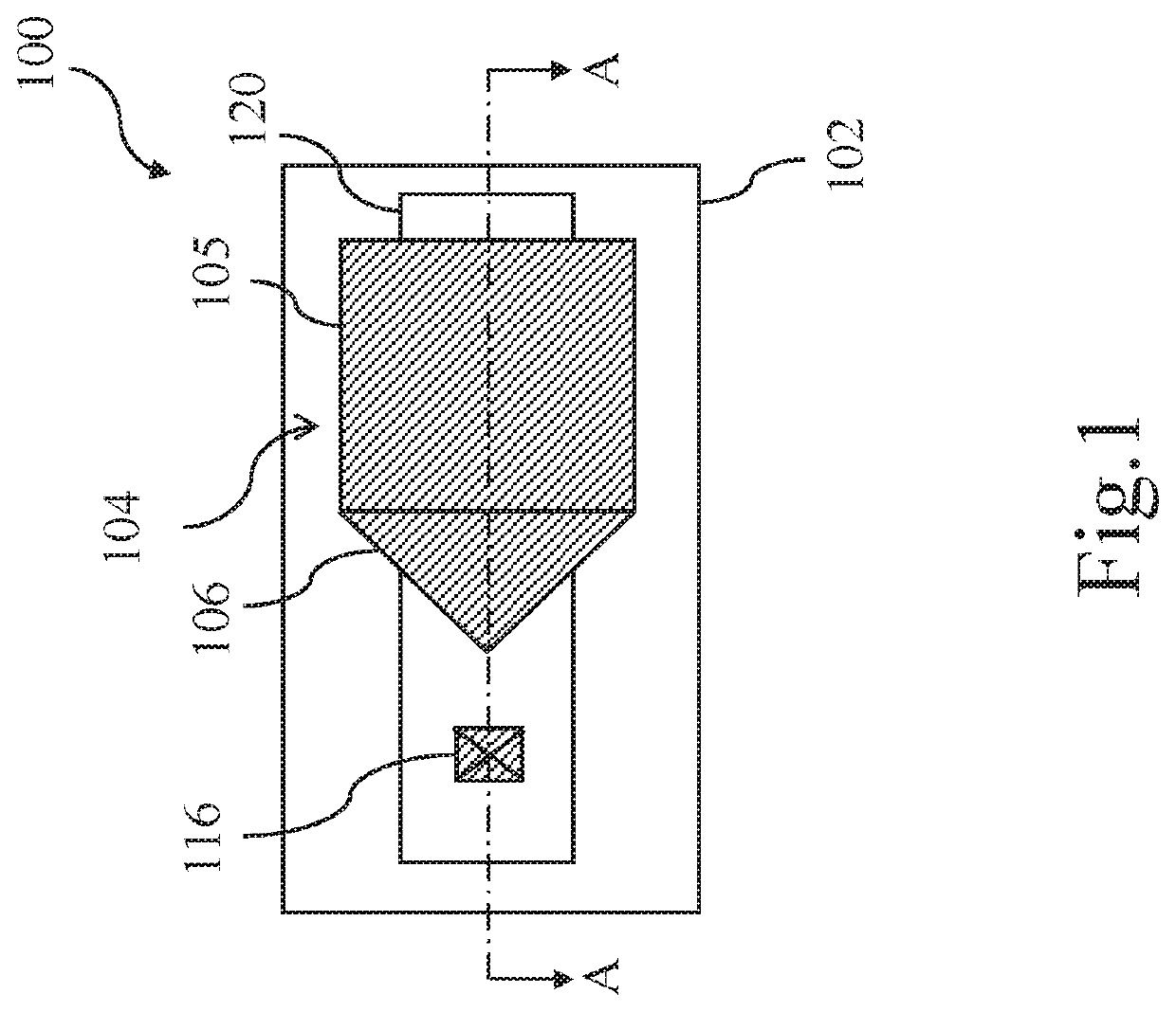
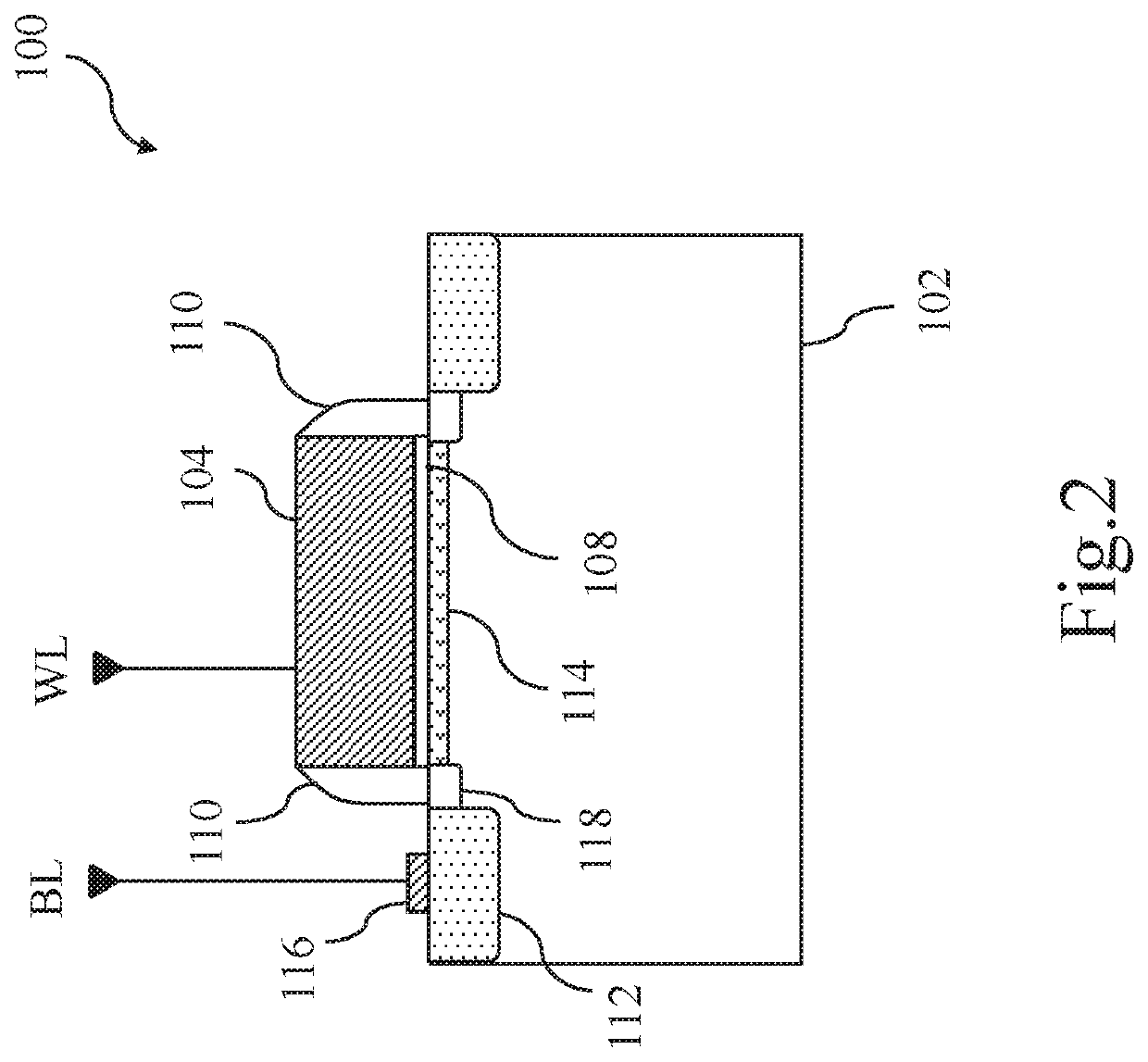
[0017]Please refer to FIG. 1, which shows a plan view of a low-voltage anti-fuse element according to a first embodiment of the present invention. Meanwhile, please refer to FIG. 2, which shows a cross-sectional view of the low-voltage anti-fuse element taken along a line A-A of FIG. 1.

[0018]In this embodiment, the low-voltage anti-fuse element 100 includes a substrate 102, a first gate 104, a first gate dielectric layer 108, a sidewall spacer 110, a first ion-doped region 112, and a channel region 114, and a bit line contact 116. The first gate dielectric layer 108 is formed on the substrate 102, the first gate 104 is stacked on the first gate dielectric layer 108, and the sidewall spacers 110 are disposed on both sides of the first gate 104. The first ion-doped region 112 is formed in the substrate 102 on one side of the first gate dielectric layer 108 and may have a lightly doped diffusion (LDD) region 118 adjacent to a vertical edge of the first gate dielectric layer 108. The fi...


PUM

PropertyMeasurementUnit
dielectricaaaaaaaaaa
electric fieldaaaaaaaaaa
voltageaaaaaaaaaa

Abstract

A low-voltage anti-fuse element is provided with a first gate dielectric layer and a first gate sequentially disposed on a substrate. A first ion-doped region is formed in the substrate on one side of the first gate. The first gate includes a body portion and a sharp corner portion extending and gradually reducing from one side of the body portion both adjacent to the first gate dielectric layer. During the operation, the principle of higher density of charges at sharp corners is utilized. When the write voltage is applied between the first gate and the first ion-doped region, a portion of the first gate dielectric layer below the sharp corner portion is liable to break down. Therefore, the breakdown voltage is reduced to achieve the purpose of reducing current consumption, while decreasing the gate area, the element size and production costs.

Description

[0001]This application claims priority for Taiwan (R.O.C.) patent application no. 109103372 filed on 4 Feb. 2020, the content of which is incorporated by reference in its entirely.BACKGROUND OF THE INVENTIONField of the Invention[0002]The present invention relates to a non-volatile memory, particularly to a low-voltage anti-fuse element using an improved gate structure to reduce the breakdown voltage.Description of the Related Art[0003]Non-volatile memories, such as EEPROM, EEPROM, and flash memory, which features electric programmability and erasability and would not lose its memory after power is turned off, has been widely used in electronic products in the computer and information age. However, the structure of the read-only memory or flash memory described above is relatively complicated. The reliability is relatively low, and the manufacturing cost is high. Therefore, one time programmable memory (OTP) with high reliability and low manufacturing cost can be used in many places...

Claims


Application Information

Patent Timeline
Patent Type & Authority Patents(United States)
IPC IPC(8): H01L27/112
CPCH01L27/11206H01L23/5252H10B20/367H10B20/25
Inventor WU, CHENG-YINGHUANG, YU-TINGHUANG, WEN-CHIEN
Owner YIELD MICROELECTRONICS CORP
Learn More