Magnetoresistance effect element including a Heusler alloy ferromagnetic layer in contact with an intermediate layer
a technology of ferromagnetic layer and magnetoresistance effect, which is applied in the field of magnetoresistance effect elements, can solve the problems of magnetoresistance effect and inability to achieve the expected mr ratio
- Summary
- Abstract
- Description
- Claims
- Application Information
AI Technical Summary
Benefits of technology
Problems solved by technology
Method used
Image
Examples
first embodiment
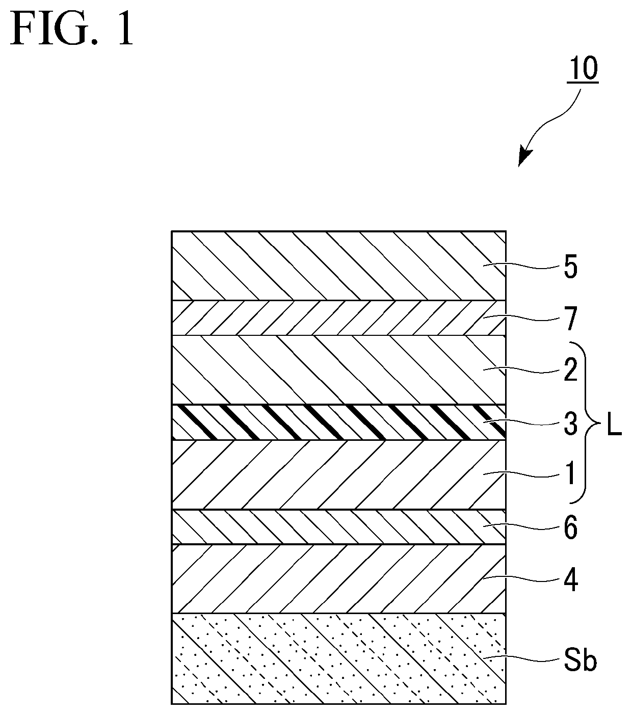
[0042]FIG. 1 is a cross-sectional view of a magnetoresistance effect element according to a first embodiment. First, directions are defined. A direction in which the respective layers are laminated on each other may be referred to as a lamination direction. Further, a direction which intersects the lamination direction and in which each of layers spreads may be referred to as an in-plane direction.
[0043]The magnetoresistance effect element 10 shown in FIG. 1 includes a substrate Sb, an underlayer 4, a protective layer 5, a laminated body L, a first intermediate layer 6, and a second intermediate layer 7.
[0044]The substrate Sb may be a crystalline substrate or an amorphous substrate. The crystalline substrate is, for example, a metal oxide single crystal, a silicon single crystal, a sapphire single crystal, or a ceramic. The amorphous substrate is, for example, a silicon single crystal with a thermal oxide film, glass, or quartz. When the substrate Sb is amorphous, an influence of a ...
example 1
[0127]The magnetoresistance effect element 10 shown in FIG. 1 was manufactured with the following configuration.
[0128]Substrate Sb: MgO single crystal substrate, thickness 0.5 mm
[0129]Underlayer 4: Ag layer, thickness 100 nm
[0130]First intermediate layer 6: Fe0.50Ga0.16Ge0.34 layer, thickness 1.1 nm
[0131]First ferromagnetic layer 1: Co2Fe1.03Ga0.41Ge0.86 layer, thickness 10 nm
[0132]Non-magnetic layer 3: Ag layer, thickness 5 nm
[0133]Second ferromagnetic layer 2: Co2Fe1.03Ga0.41Ge0.86 layer, thickness 8 nm
[0134]Second intermediate layer 7: Fe0.45Ga0.11Ge0.44 layer, thickness 0.56 nm
[0135]Protective layer 5: Ru layer, thickness 5 nm
[0136]First, the underlayer 4 was formed on the substrate Sb by a sputtering method. The substrate Sb on which the underlayer 4 was formed was heated at 250° C. for 30 minutes, and was then cooled to room temperature. After the cooling, the first intermediate layer 6 was formed on the underlayer 4 formed on the substrate Sb by a sputtering method.
[0137]Then...
example 2
[0144]Example 2 is different from Example 1 in that it includes the first interlayer 8 and the second interlayer 9. The element configuration of the magnetoresistance effect element of Example 2 is the same as the configuration shown in FIG. 5. The first interlayer 8 has a composition of Fe0.50Ga0.16Ge0.34 and a thickness of 1.1 nm. The second interlayer 9 has a composition of Fe0.45Ga0.11Ge0.44 layer and a thickness of 0.56 nm.
[0145]Other conditions were the same as in Example 1. The MR ratio of the magnetoresistance effect element of Example 2 was 31%.
PUM
 Abstract
Description
Claims
Application Information


