
Eureka
For R&D, Eureka makes reading and utilizing patents & technical documents easy.
Eureka AIR
Designed for self-driven R&D workflows. Generate viable solutions, solve complex R&D challenges, empower your innovation with AI.

Eureka Materials
Designed for material experts only. Revolutionize your material R&D, from search, analyze, to developing new materials.

TechResearch
Generate reliable direction feasibility study reports for your R&D in just a few steps.

TechSeek
Discover and master advanced knowledge NOW. Basics, ideas, possibilities, all at once.

TechMind
As an expert in R&D Theories, TechMind can generates customized viable solutions instantly.

TechRisk
Analyze your overall solution with one click, know your potential R&D risks in advance.

TechMonitor
Get weekly tech updates, stay abreast of the latest tech innovations and key insights.
Low pressure vapor phase deposition of organic thin films
- Summary
- Abstract
- Description
- Claims
- Application Information
AI Technical Summary
Benefits of technology
Problems solved by technology
Method used
Image

Examples
example 1
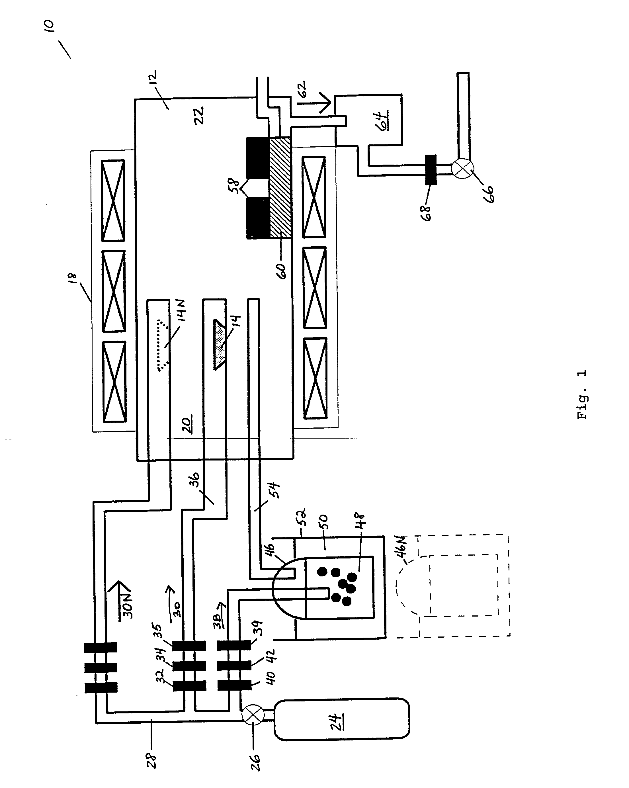
[0042] Using the apparatus of FIG. 1, layers of organic light emitting materials were grown using glass and flexible polyester substrates precoated with transparent layers of indium tin oxide (ITO). The ITO forms the anode of the device with a thickness of 1700 .ANG. and 1200 .ANG. for the glass and polyester substrates, respectively, yielding anode resistances of 10 .OMEGA. and 60 .OMEGA., respectively. Glass substrates were cleaned by rinsing in a solution of detergent and deionized water in an ultrasonic bath, and then boiling in 1,1,1-trichloroethane, rinsing in acetone and finally rinsing in 2-propanol. To avoid damage due to exposure to organic solvents, the flexible substrates were cleaned by rinsing only in the detergent and 2-propanol solutions.
[0043] Glass substrates were placed within the reactor tube 12 at a location where the temperature was approximately 220.degree. C. The first layer deposited on the ITO surface was TPD, a hole transporting material. Specifically, TPD...
example 2
[0047] An NLO film was prepared using the apparatus shown in FIG. 1. MT 48 was loaded into a 30 cm.sup.3 bubbler 46, the temperature of which was maintained at approximately 80.degree.-100.degree. C. by silicone oil bath 50. Nitrogen gas was used to bubble through the MT 48, thereby carrying MT vapor through glass tube 54 and into reactor tube 12 at a location approximately 5 cm beyond crucible 14, which contained was placed on the floor of reactor tube 12 and DASI. The pressure within reactor tube 12 was maintained at about 10.sup.-2 torr. DAS vapor reacted with the MT vapor to form a solid film of DAST on substrates 58, which were supported on substrate block 60. Excess unreacted MT vapor and any volatile side-reaction products were exhausted from exhaust tube 62. DAST films thus formed are useful as optical switches, for example.
PUM
| Property | Measurement | Unit |
|---|---|---|
| Temperature | aaaaa | aaaaa |
| Thickness | aaaaa | aaaaa |
| Pressure | aaaaa | aaaaa |
Abstract
Description
Claims
Application Information
 - R&D Engineer
- R&D Manager
- IP Professional
- Industry Leading Data Capabilities
- Powerful AI technology
- Patent DNA Extraction
Browse by: Latest US Patents, China's latest patents, Technical Efficacy Thesaurus, Application Domain, Technology Topic, Popular Technical Reports.
© 2024 PatSnap. All rights reserved.Legal|Privacy policy|Modern Slavery Act Transparency Statement|Sitemap|About US| Contact US: help@patsnap.com