
Plating apparatus and method

a technology of thin film and plating method, which is applied in the direction of electrolysis process, electrolysis components, semiconductor devices, etc., can solve the problems of increasing the cost of ic fabrication, increasing the cost of pvd or cvd tools, and increasing the cost of cu seed layer

Inactive Publication Date: 2001-11-15
ACM RES
View PDF9 Cites 102 Cited by
  • Summary
  • Abstract
  • Description
  • Claims
  • Application Information

AI Technical Summary

Benefits of technology

[0014] It is a further object of the invention to provide a novel method and apparatus for plating a thin film with an improved gap filling capability across a wafer.
[0019] It is a further object of the invention to provide a novel method and apparatus for plating copper with a low stress and good adhesion.
[0022] It is a further object of the invention to provide a novel plating system with a low cost of ownership.
[0032] It is a further object of the invention to provide a novel plating system with high productivity having a large mean time between failures (MTBF), small scheduled down time, and large equipment uptime.
[0037] In another aspect of the invention, an apparatus for plating a film on a substrate in accordance with the invention includes a substrate holder for positioning the substrate for contact with a plating electrolyte. The apparatus has at least two anodes for supplying plating current to the substrate and at least one flow controller connected to supply electrolyte contacting the substrate. At least one control system is coupled to the at least two anode and the at least one flow controller to provide electrolyte and plating current in combination to successive portions of the substrate to provide a continuous, uniform thickness film on the substrate by successive plating of the film on the portions of the substrate.
[0040] In still another aspect of the invention, an apparatus for plating a film on a substrate, includes a substrate holder for positioning the substrate in a body of electrolyte. At least one movable jet anode supplies plating current and electrolyte to the substrate. The movable jet anode is movable in a direction parallel to the substrate surface. A flow controller controls electrolyte flowing through the movable jet anode. At least one control system is coupled to the movable jet anode and the flow controller to provide electrolyte and plating current in combination to successive portions of the substrate to provide a continuous, uniform thickness film on the substrate by successive plating of the film on the portions of the substrate.

Problems solved by technology

PVD Cu deposition typically has a cusping problem which results in voids when filling small gaps (<0.18 .mu.m) with a large aspect ratio.
Another important factor is the cost; the cost of electroplating tools is two thirds or half of that of PVD or CVD tools, respectively.
As mentioned before, however, PVD Cu typically has a cusping problem, which results in voids when filling small gaps (<0.18 .mu.m) with a large aspect ratio with subsequent Cu electroplating.
As device feature size shrinks this Cu seed layer will become a more serious problem.
Also, deposition of a Cu seed layer adds an additional process, which increases IC fabrication cost.
Another disadvantage of the prior art is that the plating current and electrolyte flow pattern are manipulated dependently, or only the plating current is manipulated.
This limits the process tuning window, because the optimum plating current condition does not necessarily synchronize with optimum electrolyte flow condition for obtaining excellent gap filling capability, thickness uniformity and electrical uniformity as well as grain size and structure uniformity all at the same time.
Another disadvantage of the prior art is that plating head or plating systems are bulky with large foot prints, which causes higher cost of ownership for users.

Method used


Image

  • Plating apparatus and method
  • Plating apparatus and method
  • Plating apparatus and method

Examples


second embodiment

[0109] FIG. 13A is a plan view of a portion of a plating apparatus in accordance with the invention.

[0110] FIG. 13B is a view, partly in cross section, taken along the line 13B-13B in FIG. 13A, and partly in block diagram form, of the second embodiment of a plating apparatus in accordance with the invention.

third embodiment

[0111] FIG. 14A is a plan view of a portion of a plating apparatus in accordance with the invention.

[0112] FIG. 14B is a view, partly in cross section, taken along the line 14B-14B in FIG. 14A, and partly in block diagram form, of the third embodiment of a plating apparatus in accordance with the invention.

fourth embodiment

[0113] FIG. 15A is a plan view of a portion of a plating apparatus in accordance with the invention.

[0114] FIG. 15B is a view, partly in cross section, taken along the line 15B-15B in FIG. 15A, and partly in block diagram form, of the fourth embodiment of a plating apparatus in accordance with the invention.


PUM

PropertyMeasurementUnit
tilting angleaaaaaaaaaa
temperaturesaaaaaaaaaa
sizeaaaaaaaaaa

Abstract

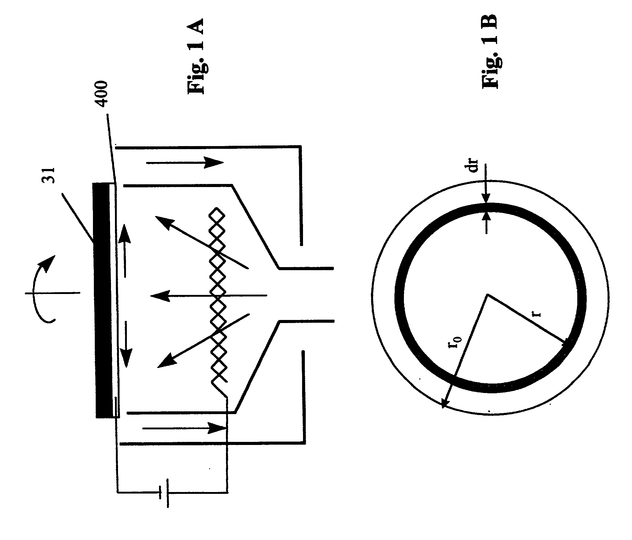
An apparatus for plating a conductive film directly on a substrate with a barrier layer on top includes anode rod (1) placed in tube (109), and anode rings (2), and (3) placed between cylindrical walls (107) and (105), (103) and (101), respectively. Anodes (1), (2), and (3) are powered by power supplies (13), (12), and (11), respectively. Electrolyte (34) is pumped by pump (33) to pass through filter (32) and reach inlets of liquid mass flow controllers (LMFCs) (21), (22), and (23). Then LMFCs (21), (22) and (23) deliver electrolyte at a set flow rate to sub-plating baths containing anodes (3), (2) and (1), respectively. After flowing through the gap between wafer (31) and the top of the cylindrical walls (101), (103), (105), (107) and (109), electrolyte flows back to tank (36) through spaces between cylindrical walls (100) and (101), (103) and (105), and (107) and (109), respectively. A pressure leak valve (38) is placed between the outlet of pump (33) and electrolyte tank (36) to leak electrolyte back to tank (36) when LMFCs (21), (22), (23) are closed. A wafer (31) held by wafer chuck (29) is connected to power supplies (11), (12) and (13). A drive mechanism (30) is used to rotate wafer (31) around the z axis, and oscillate the wafer in the x, y, and z directions shown. Filter (32) filters particles larger than 0.1 or 0.2 mum in order to obtain a low particle added plating process.

Description

[0001] 1. Field of the Invention[0002] The present invention relates generally to a method and apparatus for plating thin films and, more particularly, plating metal films to form interconnects in semiconductor devices.[0003] 2. Description of the Prior Art[0004] As semiconductor device features continue to shrink according to Moore's law, interconnect delay is larger than device gate delay for 0.18 .mu.m generation devices if aluminum (Al) and SiO2 are still being used. In order to reduce the interconnect delay, copper and low k dielectric are a possible solution. Copper / low k interconnects provide several advantages over traditional Al / SiO2 approaches, including the ability to significantly reduce the interconnect delay, while also reducing the number of levels of metal required, minimizing power dissipation and reducing manufacturing costs. Copper offers improved reliability in that its resistance to electromigration is much better than aluminum. A variety of techniques have been...

Claims


Application Information

Patent Timeline
Patent Type & Authority Applications(United States)
IPC IPC(8): C25D5/02C25D5/08C25D5/18C25D7/12C25D21/12H01L21/288H01L21/48
CPCC25D5/026C25D5/08H01L21/4846C25D21/12C25D5/18C25D5/02
Inventor WANG, HUI
Owner ACM RES
Learn More