

Ball grid array package and a packaging process for same
a technology of grid array and packaging process, which is applied in the direction of semiconductor devices, semiconductor/solid-state device details, electrical apparatus, etc., can solve the problems of low thermal dissipation efficiency, inability to provide a good route, and affecting device performan
- Summary
- Abstract
- Description
- Claims
- Application Information
AI Technical Summary
Benefits of technology
Problems solved by technology
Method used
Image

Examples
Embodiment Construction
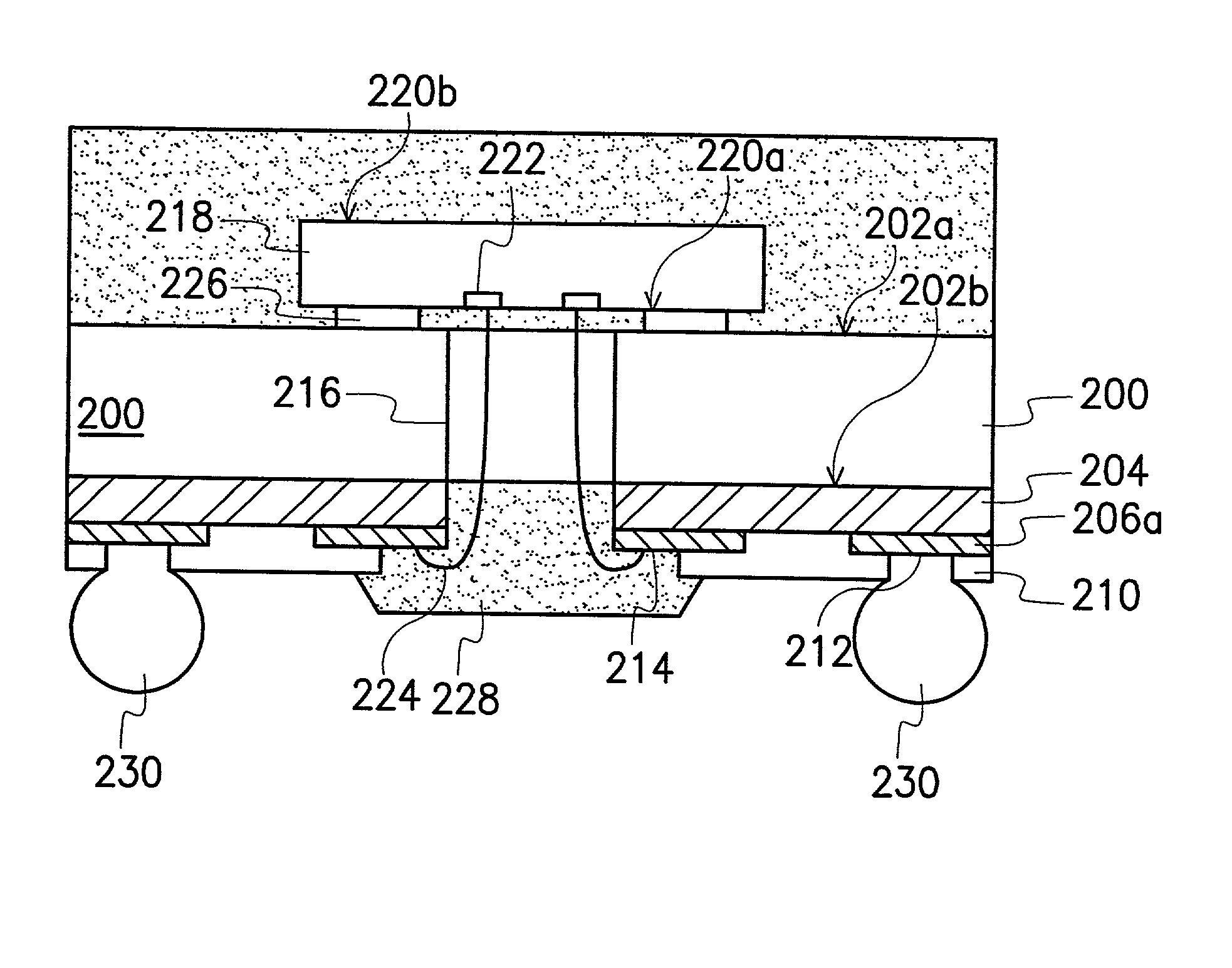
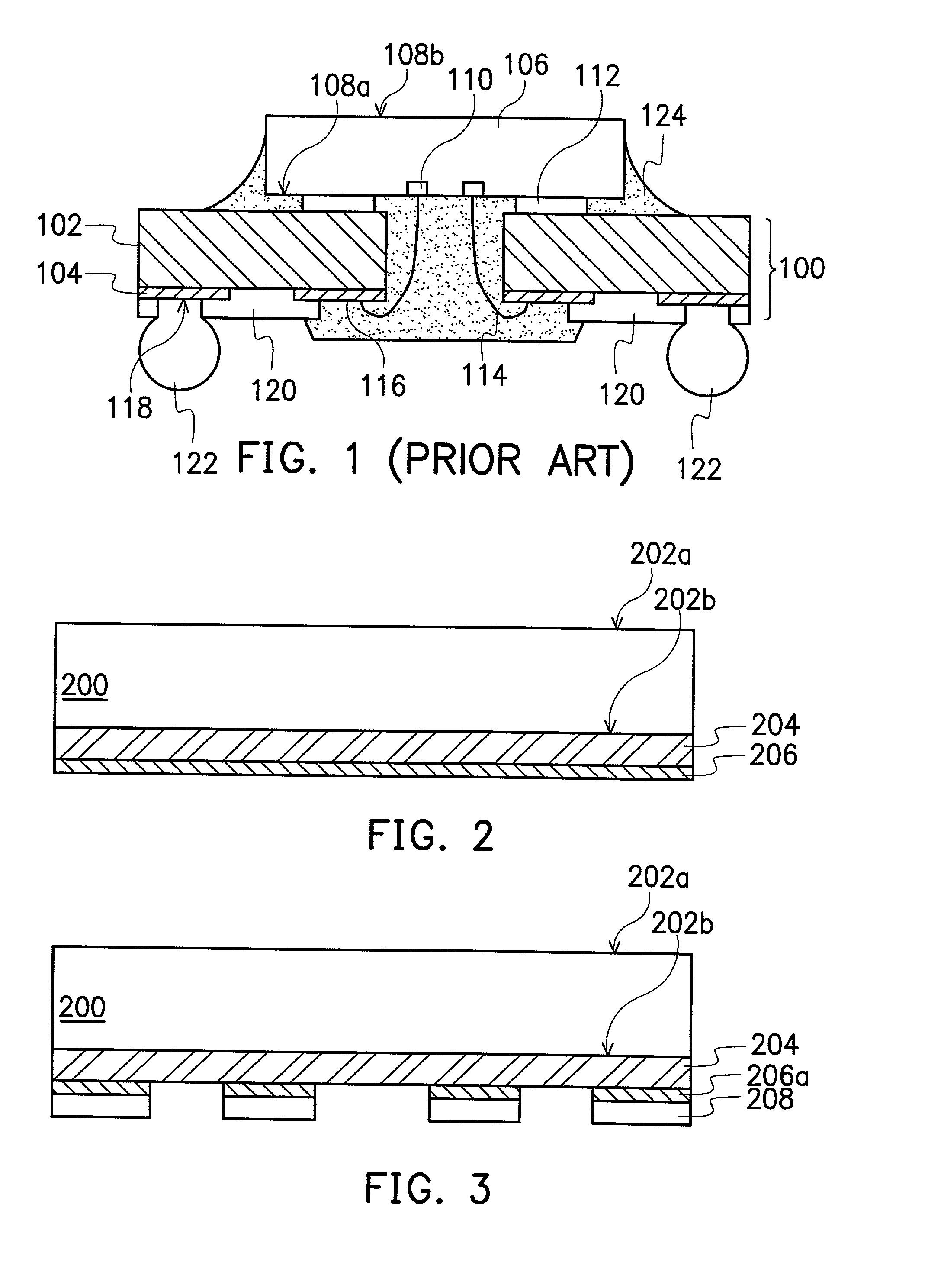
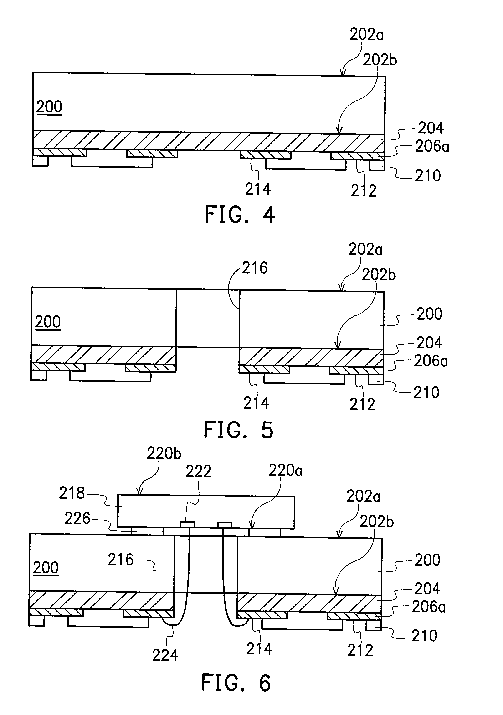
[0018] Shown in FIG. 2 to FIG. 7 are the schematic cross-sectional views illustrating the packaging process of a ball grid array in accordance with a preferred embodiment of the present invention. In FIG. 2, a thermal dissipation substrate 200 having a first surface 202a and a second surface 202b is provided. The thermal dissipation substrate 200 is made of a metal material such as copper, etc. having good heat conduction. On the second surface 202b, an insulating layer 204 and a copper foil 206 are sequentially built up. The material of the insulating layer 204 includes prepreg such as FR-4 and FR-5, Bismaleimide-Triazine (BT) or epoxy. The insulating layer 204 and the copper foil 206 can be built up on the thermal dissipation substrate 200 by pressing. The insulating layer 204 can also be formed on the second surface 202b by coating while the copper foil 206 can also be formed by plating or electroless plating. In order to enhance the bonding effect between the second surface 202b...
PUM
 Abstract
Description
Claims
Application Information