Plasma processing apparatus and method with controlled biasing functions

Inactive Publication Date: 2002-03-14
HITACHI LTD
View PDF4 Cites 29 Cited by
  • Summary
  • Abstract
  • Description
  • Claims
  • Application Information

AI Technical Summary

Benefits of technology

0011] It is the second object of the invention to provide a plasma proc

Problems solved by technology

In the above plasma processing apparatus, since the electric path of the RF power supplied to the sample to be processed propagates to cross the magnetic field, the impedance of the plasma perpendicular to this magnetic field may act to form a potential distribution in the surface of the sample to be processed, which causes charging damage.
In addition, the energy of ions incident to the sample to be processed is determined by the self-bias potential due to the biasing power fed to the sample to be processed, and there is the problem that the efficiency of the bias application is reduced since the rate of the earth area to the substrate electrode is decreased with the increase of the wafer size toward a large diameter.
Also, in the conventional apparatus, sin

Method used


Image

  • Plasma processing apparatus and method with controlled biasing functions
  • Plasma processing apparatus and method with controlled biasing functions
  • Plasma processing apparatus and method with controlled biasing functions

Examples


Embodiment Construction

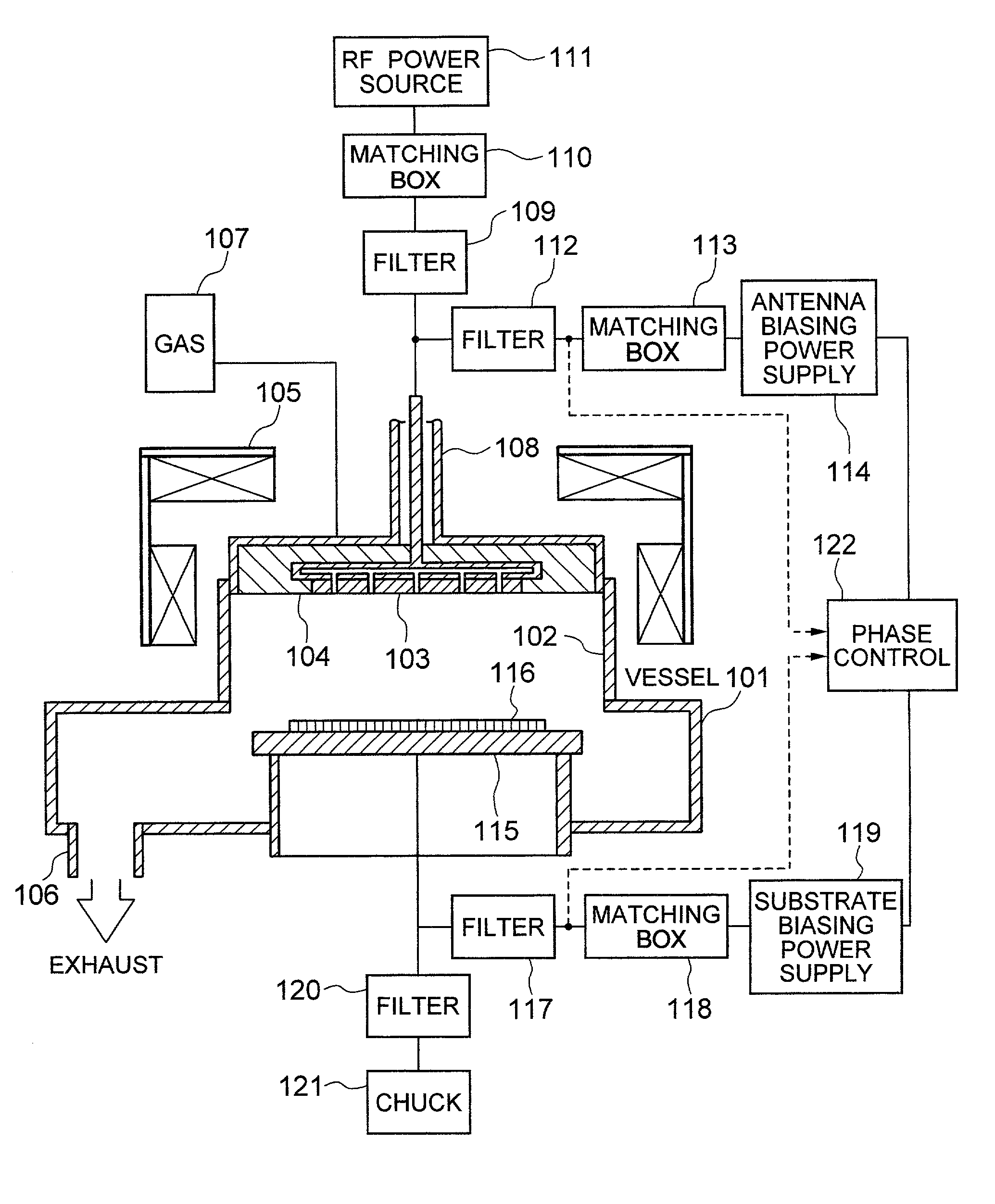
[0047] One embodiment of the invention will be described with reference to FIGS. 1 through 5. FIG. 1 is a longitudinally cross-sectional diagram of the etching apparatus as an example of the plasma processing apparatus to which the present invention is applied. A vacuum vessel 101 has provided on the upper opening side a cylindrical process container 102, a flat-shaped antenna electrode 103 of a conductor and a dielectric window 104 through which electromagnetic waves can be transmitted, so as to hermetically seal the top opening to form a process chamber inside the container. A field-producing coil 105 is provided around the outside of the process container 102 to surround the process chamber. The antenna electrode 103 has a perforated structure for the supply of etching gas from a gas feed unit 107 connected to the antenna electrode. In addition, below the vacuum vessel 101 there is provided a vacuum exhauster (not shown) that is connected via a vacuum vent 106 to the vessel.

[0048...


PUM

PropertyMeasurementUnit
Angleaaaaaaaaaa
Angleaaaaaaaaaa
Electric potential / voltageaaaaaaaaaa

Abstract

Processing technique using plasma to process the surface of a sample such as semiconductor device. The phases of RF bias voltages applied to a substrate electrode and an antenna electrode opposed thereto are controlled to be opposite to each other so that either one of the electrodes is forced to always function as ground. Therefore, the current flowing to cross the magnetic field for controlling the plasma is decreased, and the potential distribution difference in the surface of the sample to be processed is reduced, so that the charging damage can be suppressed. Energy of ions incident to the sample to be processed can be controlled to perform high-precision etching. The plasma potential can also be controlled so that the strength of the ion impact to the inner wall of the chamber can be reduced, thereby reducing particles detached from the inner wall of the processing apparatus to improve the throughput.

Description

[0001] 1. Field of the Invention[0002] The present invention relates to plasma processing apparatus and method, and particularly to a plasma processing apparatus and method suitable for making surface treatment of a sample such as a semiconductor device by use of plasma.[0003] 2. Description of the Related Art[0004] In the plasma etching process, the processing gas is ionized to be activated for fast processing, and radio frequency (RF) biasing power is supplied to a sample to be processed (or a processed sample) so that the ions in the plasma can be incident perpendicularly to the sample to be processed, thereby achieving high-precision etching for anisotropic shape and so on.[0005] A plasma processing apparatus for this purpose is disclosed in Yokogawa et al U.S. Pat. No. 5,891,252. This apparatus, as described in that document, has an air-core coil provided on the outer periphery of the outside of a vacuum vessel, and a circular conductor plate provided to oppose a wafer stage wi...

Claims


Application Information

Patent Timeline
IPC IPC(8): C23C16/44C23C16/50C23C16/509
CPCC23C16/4401C23C16/5096H01J37/32165
Inventor SUMIYA, MASAHIROYASUI, NAOKIWATANABE, SEIICHI
Owner HITACHI LTD
Why Eureka
Try Eureka