Electron emission device, cold cathode field emission device and method for the production thereof, and cold cathode field emission display and method for the production thereof

Inactive Publication Date: 2002-03-28
SONY CORP
View PDF2 Cites 69 Cited by
  • Summary
  • Abstract
  • Description
  • Claims
  • Application Information

AI Technical Summary

Benefits of technology

0117] In the present invention, the electron emitting portion composed of the carbon film is formed on the carbon film selective-growth region. In this case, a kind of catalytic reaction is expected on the surface of the carbon film selective-growth region, the formation of seeds or nuclei at an initial stage of the carbon film formation proceeds smoothly, the formation of seeds or nuclei promotes the growth of the carbon film thereafter, and the electron emitting portion composed of the carbon film can be formed in a desired portion of the conductive layer or the cathode electrode. Further, it is no longer necessary to pattern the carbon film for bringing the carbon fil

Problems solved by technology

For applying the liquid crystal display to a floor-type television receiver, however, it still has problems to be solved concerning a higher brightness and an increase in size.
Further, when oxygen gas is used as an etching gas, the resist layer is worn to a great extent.
For these reasons, in the conventional oxygen plasma process of a diamond thin film, the pattern transfer difference of the diamond thin fi

Method used


Image

  • Electron emission device, cold cathode field emission device and method for the production thereof, and cold cathode field emission display and method for the production thereof
  • Electron emission device, cold cathode field emission device and method for the production thereof, and cold cathode field emission display and method for the production thereof
  • Electron emission device, cold cathode field emission device and method for the production thereof, and cold cathode field emission display and method for the production thereof

Examples


example 2

[0156] Example 2 is directed to variants of the electron emission device and the display explained in Example 1. In the production method explained in Example 1, the metal particles 21 are allowed to adhere onto the surface of the cathode electrode portion. In Example 2, the step of forming a carbon film selective-growth region comprises the step of forming a metal thin layer composed of titanium (Ti) by a sputtering method. The method for the productions of the electron emission device and the display in Example 2 will be explained below with reference to FIGS. 5A and 5B.

[0157] [Step-200]

[0158] A cathode electrode 11 is formed on a supporting substrate 10 made, for example, of glass in the same manner as in [Step-100] in Example 1. Then, a resist material layer is formed on the entire surface by a spin coating method, and then, a mask layer composed of the resist material layer is formed by lithography so as to expose a surface of the cathode electrode portion.

[0159] [Step-210]

[016...

example 3

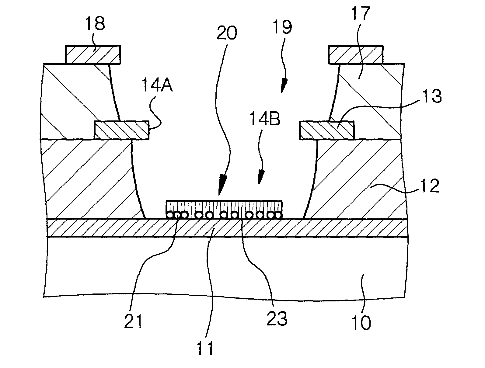
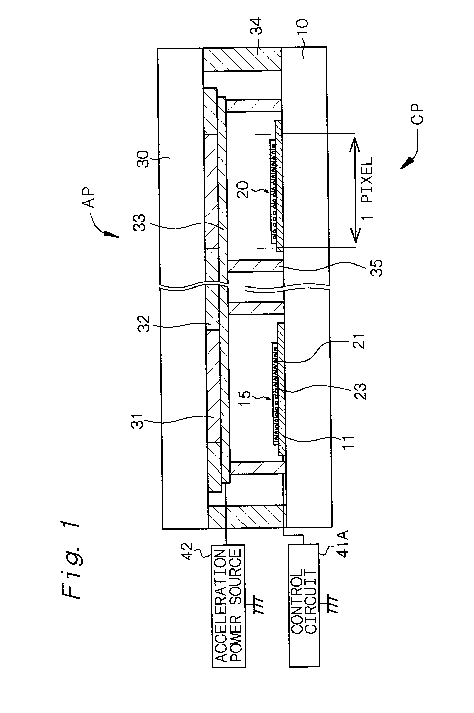
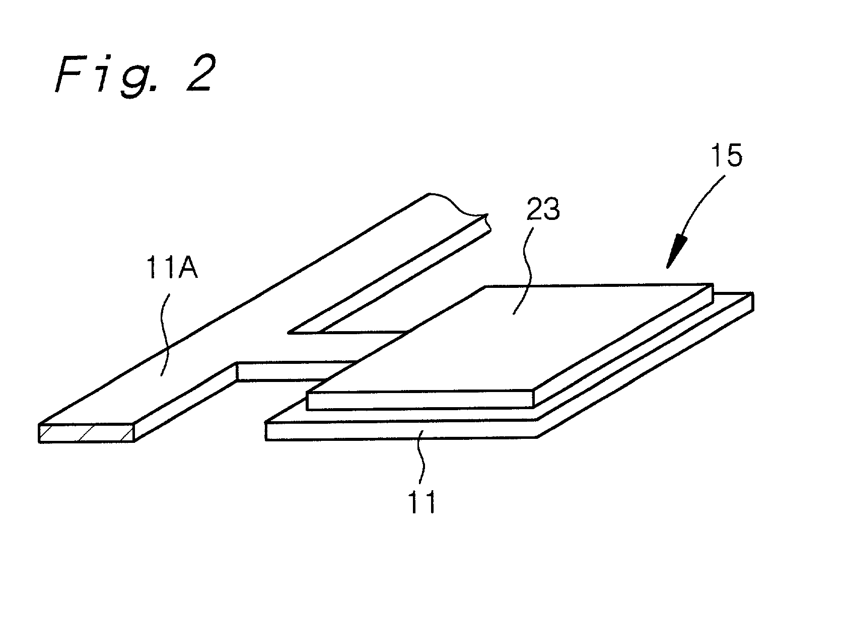
[0162] Example 3 is directed to the cold cathode field emission device (to be abbreviated as "field emission device" hereinafter) according to the first aspect of the present invention and the display according to the second aspect of the present invention.

[0163] FIG. 6 shows a schematic partial end view of the display, of Example 3. FIG. 7B shows a basic constitution of the field emission device. The field emission device of Example 3 has a cathode electrode 11 formed on a supporting substrate 10 and a gate electrode 13 which is formed above the cathode electrode 11 and has an opening portion (first opening portion 14A). The field emission device further has an electron emitting portion 15 composed of a carbon film 23 formed on a surface of a portion of a cathode electrode 11 which portion is positioned in a bottom portion of the opening portion 14A. An insulating layer 12 is formed on the supporting substrate 10 and the cathode electrode 11, and an opening portion 14B communicatin...

example 4

[0180] Example 4 is a variant of Example 3. In the production method for each of the field emission device and the display explained in Example 3, the surface of the cathode electrode 11 is naturally oxidized, so that it is sometimes difficult to form the carbon film 23. In Example 4, the metal oxide (so-called natural oxide film) is removed from the surface of the cathode electrode portion. The metal oxide on the surface of the cathode electrode portion can be removed by plasma reduction treatment or washing.

[0181] The field emission device and the display to be produced in Example 4 or Example 5 to be described later are structurally the same as those in Example 3, so that detailed explanations thereof are omitted. The method for the production of the field emission device and the display in Example 4 will be explained below.

[0182] [Step-400]

[0183] First, in the same manner as in [Step-300] to [Step-320] in Example 3, a cathode electrode 11 is formed on a supporting substrate 10 m...


PUM


Abstract

A cold cathode field emission device comprising (a) a cathode electrode formed on a supporting substrate, and (b) a gate electrode which is formed above the cathode electrode and has an opening portion, and further comprising (c) an electron emitting portion composed of a carbon film formed on a surface of a portion of the cathode electrode which portion is positioned in a bottom portion of the opening portion.

Description

BACKGROUND OF THE INVENTION AND RELATED ART STATEMENT[0001] The present invention relates to an electron emission device for emitting electrons from a carbon film, a cold cathode field emission device having an electron emitting portion composed of a carbon film and a method for the production thereof, and it also relates to a cold cathode field emission display having such cold cathode field emission devices and a method for the production thereof.[0002] In the fields of displays for use in television receivers and information terminals, studies have been made for replacing conventionally mainstream cathode ray tubes (CRT) with flat-panel displays which are to comply with demands for a decrease in thickness, a decrease in weight, a larger screen and a high fineness. Such flat panel displays include a liquid crystal display (LCD), an electroluminescence display (ELD), a plasma display panel (PDP) and a cold cathode field emission display (FED). Of these, a liquid crystal display is ...

Claims


Application Information

Patent Timeline
IPC IPC(8): H01J1/30H01J1/304H01J9/02H01J31/15
CPCH01J1/304H01J9/025H01J2201/319H01J1/30H01J9/02H01J31/15
Inventor MUROYAMA, MASAKAZUSAITO, ICHIROINOUE, KOUJIYAGI, TAKAO
Owner SONY CORP
Why Eureka
Try Eureka