

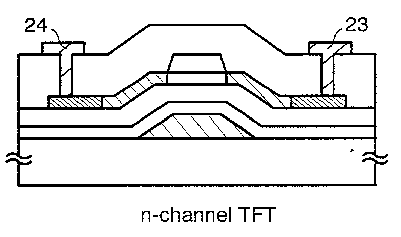
Semiconductor device
a technology of semiconductors and semiconductors, applied in semiconductor devices, electrical devices, transistors, etc., can solve the problems of increasing the energy consumed during the manufacturing process, difficult to obtain uniform crystals across a wide surface area, and inability to consider the suitable processing temperature and processing tim
- Summary
- Abstract
- Description
- Claims
- Application Information
AI Technical Summary
Problems solved by technology
Method used
Image

Examples
embodiment 1
[0149] [Embodiment 1]
[0150] An example of manufacturing an n-channel reverse stagger TFT is explained below using FIGS. 14A to 14F.
[0151] A substrate 11 is first prepared. An insulating substrate such as glass substrate, a quartz substrate, or a crystalline glass substrate can be used as the substrate 11. Note that a structure in which a base film is formed in order to prevent impurities from diffusing from the substrate, and increasing the electrical characteristics of the TFT, may also be used. If a base film is formed, a film such as a silicon oxide film, a silicon nitride film, a silicon oxynitride film (SiOxNy), or a lamination film of these films can be used with a film thickness in the range of 100 to 500 nm. Film formation methods such as thermal CVD, plasma CVD, evaporation, sputtering, and low pressure thermal CVD can be used as the film formation means. Conversely, an insulating film may be formed on the surface of a semiconductor substrate such as one of silicon, germani...
embodiment 2
[0196] [Embodiment 2]
[0197] An example of manufacturing a p-channel reverse stagger type TFT is explained below using FIGS. 21A to 21E.
[0198] Only the doping process differs in embodiment 2 from that of embodiment 1, and the other processes are identical. An explanation of the identical processes is therefore omitted.
[0199] First, similar to embodiment 1, gate insulating films 303a and 303b are formed after forming a gate wiring 302 on a substrate 301. Next, in accordance with embodiment 1, a semiconductor layer 304 is formed. (See FIG. 21A.)
[0200] An insulating layer 305 is formed next in accordance with embodiment 1. (See FIG. 21B.)
[0201] A process of adding an impurity element which imparts p-type conductivity to the semiconductor layers is performed next using the insulating layer 305 as a mask, forming impurity regions (p.sup.+ regions) 306 and 307. (See FIG. 21C.) A periodic table group 13 element, for example B, Al, Ga, In, or Tl, can be used as the impurity element which imp...
embodiment 3
[0212] [Embodiment 3]
[0213] An example of manufacturing an n-channel reverse stagger type TFT and a p-channel reverse stagger type TFT on the same substrate is explained here using FIGS. 22A to 22D and FIGS. 23A to 23C.
[0214] Only the doping process differs in embodiment 3 from that of embodiment 1, and the other processes are identical. An explanation of the identical processes is therefore omitted.
[0215] First, similar to embodiment 1, gate insulating films 403a and 403b are formed after forming gate wirings 401 and 402 on a substrate 400. Semiconductor layers 404 and 405 are formed next in accordance with embodiment 1. (See FIG. 22A.)
[0216] Insulating layers 406 and 407 are formed next in accordance with embodiment 1. (See FIG. 22B.)
[0217] A resist mask 408, which covers portions of the semiconductor layers that become an n-channel TFT, is formed using a photo mask, and a resist mask 409, which covers portions of the semiconductor layers which become a p-channel TFT, is also form...
PUM
| Property | Measurement | Unit |
|---|---|---|
| thickness | aaaaa | aaaaa |
| thickness | aaaaa | aaaaa |
| diameter | aaaaa | aaaaa |
Abstract
Description
Claims
Application Information