Solid state laser device and solid state laser device system

a laser device and laser device technology, applied in the direction of semiconductor lasers, active medium materials, instruments, etc., can solve the problems of inability to effectively excite solid state laser elements, limited element, and inability to excite laser ligh

Inactive Publication Date: 2002-05-02
MITSUBISHI ELECTRIC CORP
View PDF18 Cites 12 Cited by
  • Summary
  • Abstract
  • Description
  • Claims
  • Application Information

AI Technical Summary

Problems solved by technology

As a result, there is such a problem that the intensity of the excitation laser light, that can be irradiated to the solid state laser element, is limited by the optical output of the excitation laser, that can be output to the outside of the optical resonator of the excitation laser.
Also, there is another problem that, when the solid state laser element having a small thickness should be excited, the excitation light transmits the solid state laser element and thus it is impossible to excite effectively such solid state laser element.

Method used


Image

  • Solid state laser device and solid state laser device system
  • Solid state laser device and solid state laser device system
  • Solid state laser device and solid state laser device system

Examples


embodiment 1

[0086] (Embodiment 1)

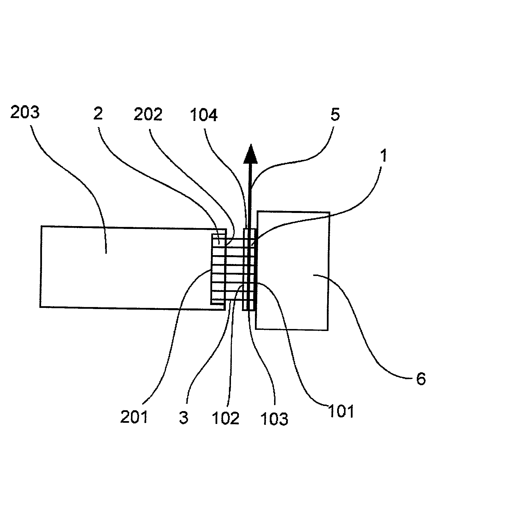
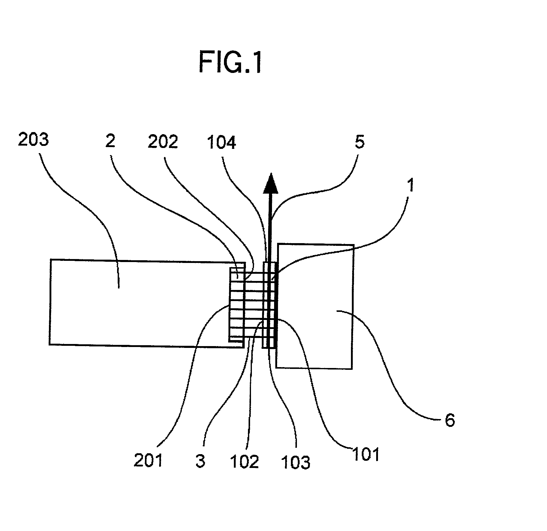
[0087] FIG. 1 is a top view showing a structure of an exciting portion of a solid state laser device according to an embodiment 1 of the present invention. In FIG. 1, 1 is a solid state laser element containing an active medium, 2 is a semiconductor laser as an excitation light source, 3 is an excitation light emitted from the semiconductor laser array, 5 is a laser light emitted from the solid state laser element 1, and 6 is a heat sink for cooling the solid state laser element. The solid state laser device of the present embodiment shows such a structure that a thin-plate Yb (Ytterbium)-doped YAG (Yttrium Aluminum Garnet) crystal, which is a three-level laser having an oscillation wavelength of 1030 nm, is employed as the solid state laser element 1.

[0088] Also, the semiconductor laser array 2 in which several tens light emitting portions are provided linearly on a single element having a length of 1 cm and which uses InGaAs (Indium Gallium Arsenide) as the ac...

embodiment 2

[0113] (Embodiment 2)

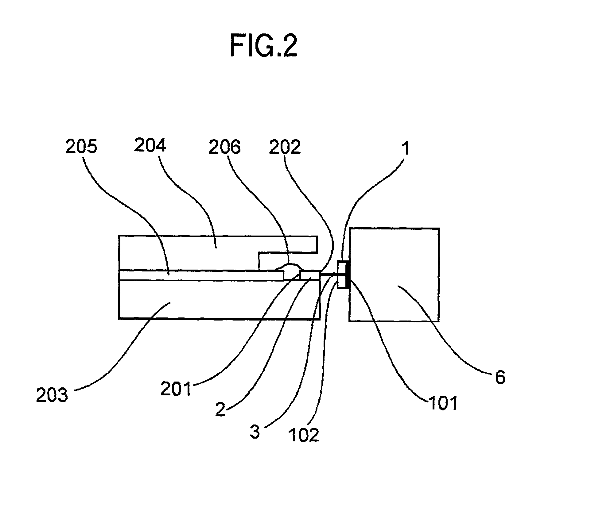
[0114] FIG. 5 is a top view showing a structure of an exciting portion of a solid state laser device according to an embodiment 2 of the present invention. In FIG. 5, the same symbols as those in FIG. 1 denote the same parts or the equivalent parts. In the solid state laser device of the present embodiment, an optical element 4 consisting of an aspherical cylindrical lens is arranged between the solid state laser element 1 and the semiconductor laser array 2.

[0115] FIG. 6 is a front view showing the structure of the exciting portion of the solid state laser device according to the embodiment 2 when viewed from the optical axis direction of the solid state laser element. In the solid state laser device of the present embodiment, like the embodiment 1, the first optical resonator is constructed by applying the high reflection coating to the oscillation wavelength of the semiconductor laser array 2 to the end face 201 of the semiconductor laser array 2 positioned o...

embodiment 3

[0119] (Embodiment 3)

[0120] FIG. 7 is a top view showing a structure of an exciting portion of a solid state laser device according to an embodiment 3 of the present invention. In the solid state laser device of the present embodiment, like the embodiment 1 or 2, the first optical resonator for the excitation light is constructed by applying the high reflection coating to the oscillation wavelength of the semiconductor laser array 2 to the end face 201 of the semiconductor laser array 2 and the side 101 of the solid state laser element 1 respectively. In FIG. 7, 401 is an optical element for correcting a mode pattern of the excitation light 3 in the direction perpendicular to the active layer of the semiconductor laser array 2 like the optical element 4 shown in the embodiment 2, and 402 is an optical element constructed by a microlens array arranged to respond to a number of light emitting portions in the semiconductor laser array 2, for correcting a mode pattern of the excitation ...


PUM

PropertyMeasurementUnit
oscillation wavelengthaaaaaaaaaa
lengthaaaaaaaaaa
oscillation wavelengthaaaaaaaaaa

Abstract

A semiconductor laser array is arranged on the side of a solid state laser element, and an optical resonator to an excitation light is constructed by applying a high reflection coating to an oscillation wavelength of the semiconductor laser array is applied to an end face of the semiconductor laser array positioned on the opposite side to the solid state laser element and a side of the solid state laser element positioned on the opposite side to the semiconductor laser array. The solid state laser element is arranged on the inside of the optical resonator, and the solid state laser element is excited optically by the excitation light.

Description

[0001] [Technical Field][0002] The present invention relates to a solid state laser device capable of generating a solid state laser light stably and effectively with a simple and inexpensive structure.[0003] [Related Art][0004] FIG. 26 is a schematic view showing a structure of the solid state laser device disclosed in Koechner, "Solid-state Laser Engineering", pp. 342 to 347 (published by Springer Verlag), for example, in the prior art. In FIG. 26, 1 is a solid state laser element containing an active medium, 2 is a semiconductor laser as an excitation light source, 3 is an excitation light emitted from the semiconductor laser array, 4 is a beam shaping optical system for converging the excitation light 3, 5 is a solid state laser light emitted from the solid state laser element 1, and 8 is a partial reflection mirror for transmitting a part of the solid state laser light.[0005] Also, 151 is a side of the solid state laser element 1 directed to the semiconductor laser 2 side, on w...

Claims


Application Information

Patent Timeline
Patent Type & Authority Applications(United States)
IPC IPC(8): H01S3/04H01S3/042H01S3/06G02F1/37H01S3/094H01S3/0941H01S3/109H01S3/113H01S3/16H01S3/23H01S5/028H01S5/40
CPCH01S3/0407H01S3/025H01S3/0604H01S3/07H01S3/08059H01S3/094084H01S3/0941H01S3/1618H01S3/1643H01S5/024H01S5/4031H01S3/0625H01S3/08095H01S3/09408H01S5/14H01S5/4062H01S3/042
Inventor FUJIKAWA, SHUICHIYASUI, KOJI
Owner MITSUBISHI ELECTRIC CORP
Why Eureka
Try Eureka