Material inspection

a technology of material inspection and inspection, applied in the direction of instruments, soldering apparatus, fluorescence/phosphorescence, etc., can solve the problems of joint reliability reduction, joint stringency, affecting joint high frequency signal propagation, etc., and achieve the effect of avoiding downstream processing defects

Inactive Publication Date: 2002-05-09
AGILENT TECH INC
View PDF0 Cites 62 Cited by
  • Summary
  • Abstract
  • Description
  • Claims
  • Application Information

AI Technical Summary

Benefits of technology

0037] In a further embodiment, the method comprises the further step of providing in-line p

Problems solved by technology

Whichever technique is used, there are very stringent requirements to be met to ensure good quality chip or circuit production, and the stringency arises particularly because of the ever-decreasing scales involved.
Voids in solder balls are in turn linked to reduction in joint reliability and they affect the joint high frequency signal propagation.
Excess flux can also interact with solder mask to cause excessive residues and increase migration between adjacent solder joints.
Meeting quality standards is often complicated by various attributes of the dielectric material.
Also, in screen printing, there is a tendency for air bubbles to be worked into the flux.
H

Method used


Image

  • Material inspection
  • Material inspection
  • Material inspection

Examples


Embodiment Construction

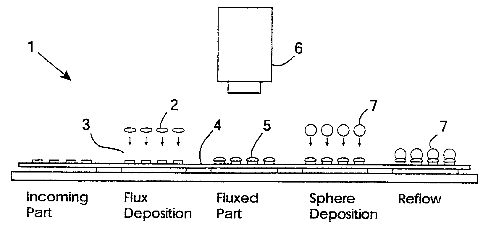
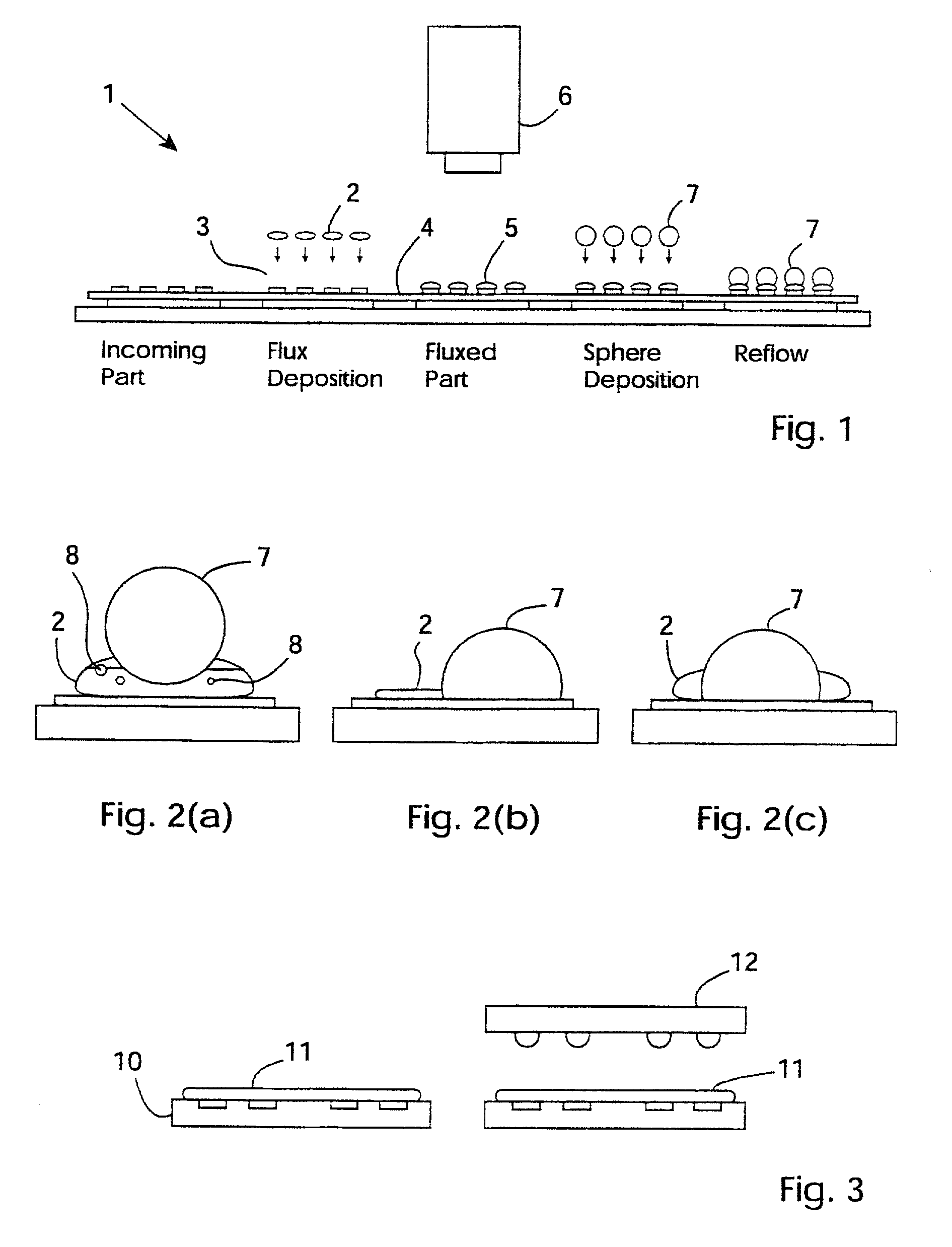
[0064] Referring to FIG. 1 a chip scale packaging (CSP) ball grid array (BGA) process 1 is described. Solder flux 2 is deposited onto conductive pads 3 on a substrate 4. Fluxed conductive pads 5 are inspected by an inspection station 6. This inspection provides detailed in-line information about the manner in which the flux 2 had been deposited. This information provides a strong indication of the likely quality of the downstream processing steps. Balls 7 of solder are then applied onto the fluxed conductive pads 5. Upon reflow, the balls 7 are soldered to the fluxed pads 5.

[0065] Referring to FIG. 2(a) excess flux 2 results in poor contact between the solder ball 7 and the pad 4 (copper, Ni / Au or other conductor). This results in poor bonding strength and poor electrical conductivity, with a likelihood of short to medium term failure. In addition, the presence of voids 8 can affect the quality of the ball attachment. As shown in FIG. 2(b), insufficient flux 2 can result in the ball...


PUM

PropertyMeasurementUnit
Timeaaaaaaaaaa
Angleaaaaaaaaaa
Angleaaaaaaaaaa

Abstract

An inspection station (6) has a ring of 370 nm LEDs (24) for low-angle diffuse illumination of flux. This stimulates inherent fluorescent emission of the flux without the need for flux additives or pre-treatment. A CCD sensor (20) detects the emission. An image processor generates output data indicating flux volume according to a relationship between emission intensity and volume over the surface of the flux. Intensity non-uniformity indicates either height non-uniformity or hidden voids, both of which give rise to defects after application of solder paste and reflow. The inspection is particularly effective for pre solder application flux inspection.

Description

[0001] The invention relates to inspection of dielectric materials used in the electronics industry such as flux on its own or in solder paste.PRIOR ART DISCUSSION[0002] Such materials are used in two main branches of the electronics industry, namely (a) surface mount technique (SMT) circuit production processes and (b) chip scale packaging (CSP).[0003] The CSP branch includes ball grid array (BGA) and flip-chip processes. In BGA processes an array of solder balls is deposited on a substrate which was previously coated with flux. The flux, when heated during the reflow process, improves the cleanliness of the resulting solder joint as well as improving the mechanical and electrical connectivity between the solder and the pad to which it is soldered. In flip-chip packaging, a solder mask covers a copper substrate to reveal an array of spots at which the copper is exposed. Flux is applied over the mask and a flip-chip having an array of balls on a lower surface is deposited onto the s...

Claims


Application Information

Patent Timeline
IPC IPC(8): G01N21/64B23K1/00B23K3/08G01N21/00G01N21/88G01N21/956
CPCB23K3/08
Inventor OWENBOYLE, ADRIANCONLON, PETER
Owner AGILENT TECH INC
Why Eureka
Try Eureka