Method for manufacturing gallium nitride compound semiconductor element and gallium nitride compound semiconductor element

a gallium nitride and compound semiconductor technology, applied in the direction of polycrystalline material growth, crystal growth process, after-treatment details, etc., can solve the problems of simple doping not producing difficult to form a p-type gan compound semiconductor, degradation of the characteristics of the light emitting elemen

Inactive Publication Date: 2002-06-06
NITRIDE SEMICON
View PDF6 Cites 4 Cited by
  • Summary
  • Abstract
  • Description
  • Claims
  • Application Information

AI Technical Summary

Problems solved by technology

However, it is generally difficult to form a P type GaN compound semiconductor.
Therefore, such simple doping does not produce a P type GaN compound semiconductor.
However, in the method of annealing at a high temperature of 700.degree. C. or greater in order to prepare a P type GaN compound semiconductor, the annealing process degrades the GaN itself, frequently resulting in degradation of the characteristics of the light emitting element.
Meanwhile, the method of irradiating an electron beam is not suited for use over large areas, and therefore is not an industrially practical approach.

Method used


Image

  • Method for manufacturing gallium nitride compound semiconductor element and gallium nitride compound semiconductor element
  • Method for manufacturing gallium nitride compound semiconductor element and gallium nitride compound semiconductor element
  • Method for manufacturing gallium nitride compound semiconductor element and gallium nitride compound semiconductor element

Examples


Embodiment Construction

[0022] A preferred embodiment of the present invention will now be described referring to the figures and with a light emitting element as an example.

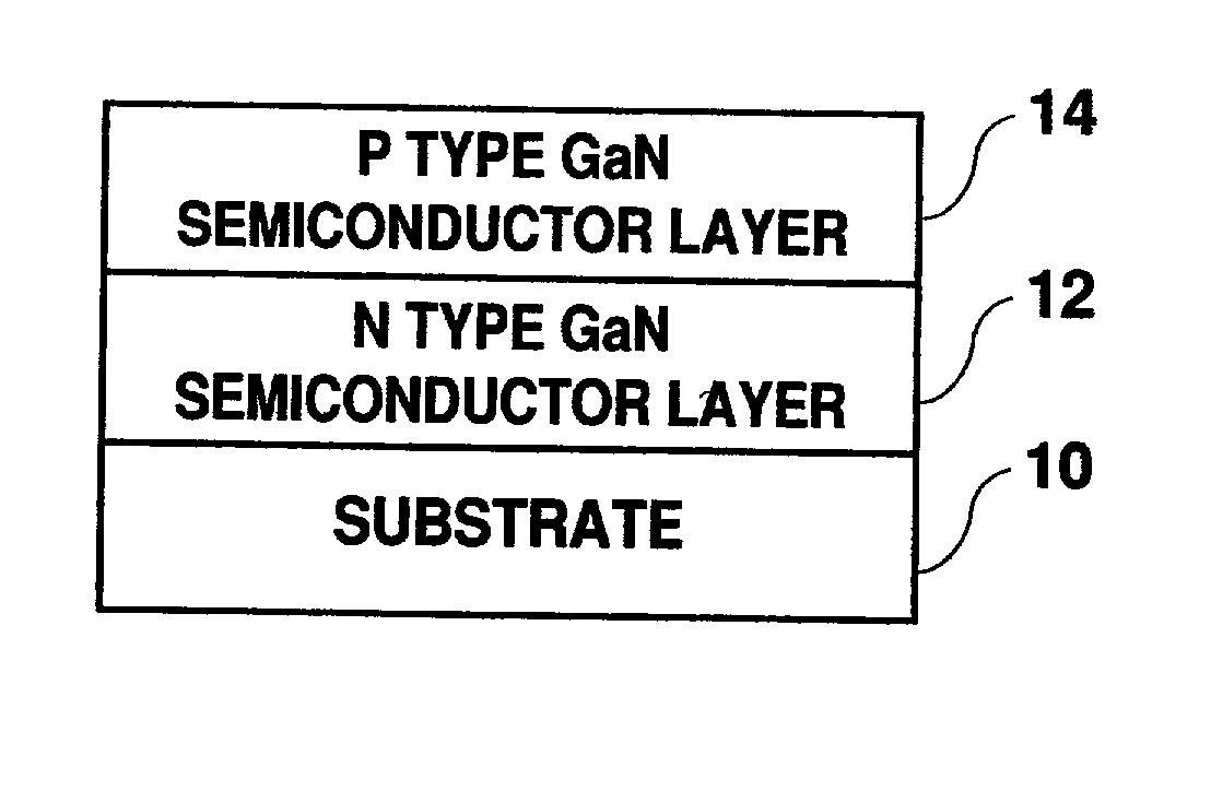
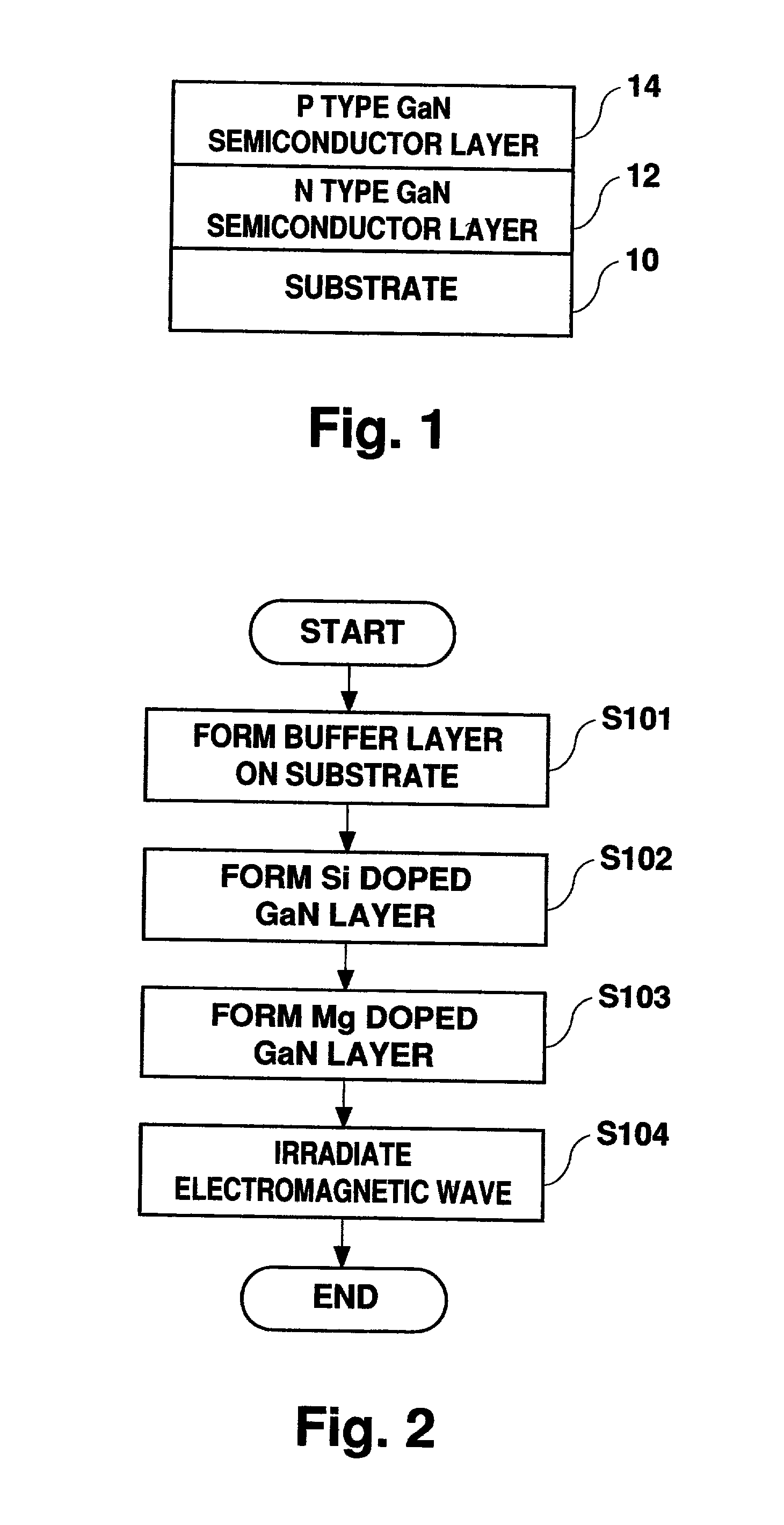
[0023] FIG. 1 shows relevant structures in a GaN compound semiconductor light emitting element (excluding electrodes etc.) which is manufactured by a method of manufacturing according to the preferred embodiment. An N type GaN compound semiconductor layer 12 is formed on a substrate 10 and a P type GaN compound semiconductor layer 14 is formed on the N type GaN compound semiconductor layer 12. Each of the layers can be formed using, for example, a MOCVD method. The N type GaN compound semiconductor layer 12 may comprise a single layer of GaN, AlGaN, or InGaN, or a laminated structure of these compounds (for example, GaN / AlGaN / InGaN including a superlattice structure (SLS etc.)), or by doping an N type impurity such as Si to these structures. When forming the N type compound semiconductor layer 12, a buffer layer may first be formed on ...


PUM

PropertyMeasurementUnit
frequencyaaaaaaaaaa
wavelengthaaaaaaaaaa
temperatureaaaaaaaaaa

Abstract

A method for obtaining a P type GaN compound semiconductor in a GaN compound semiconductor element. An N type GaN compound semiconductor layer is formed on a substrate. A GaN compound semiconductor layer to which a P type impurity is doped is formed on the N type GaN compound semiconductor layer. The GaN compound semiconductor layer to which the P type impurity is doped is irradiated with electromagnetic radiation of a predetermined wavelength to selectively agitate hydrogen bonds to dissociate H, and activate P type impurity as an acceptor.

Description

[0001] 1. Field of the Invention[0002] The present invention relates to a method for manufacturing a gallium nitride (GaN) compound semiconductor element, and in particular to a method for manufacturing a PN junction element or the like.[0003] 2. Description of the Related Art[0004] A wide variety of applications for GaN compound semiconductor LEDs emitting blue light (450 nm) or ultraviolet radiation are being considered.[0005] As a GaN compound semiconductor, AlGaN and InGaN, and a laminated structure of these compounds and GaN are being considered. In order to use the compounds for a light emitting element, a PN junction must be provided. More specifically, an N type GaN compound semiconductor and a P type GaN compound semiconductor must be formed.[0006] In order to form an N type GaN compound semiconductor, an N type impurity such as, for example, Si and Sn, can be doped. However, it is generally difficult to form a P type GaN compound semiconductor. In other words, simple dopin...

Claims


Application Information

Patent Timeline
Patent Type & Authority Applications(United States)
IPC IPC(8): C30B25/02C30B33/00H01L21/205H01L21/268H01L21/324H01L33/32
CPCC30B25/02C30B29/403H01L21/3245C30B33/00C30B29/406
Inventor SAKAI, SHIRO
Owner NITRIDE SEMICON
Why Eureka
Try Eureka