

Multi-layer Pt electrode for DRAM and FRAM with high K dielectric materials
a dielectric material and pt electrode technology, applied in the field of memory ics fabrication, can solve the problems of increasing the number and variety of processing chemicals, affecting the performance of the electrode, so as to increase the resistance of the electrode and reduce the variation of the material
- Summary
- Abstract
- Description
- Claims
- Application Information
AI Technical Summary
Benefits of technology
Problems solved by technology
Method used
Image

Examples
Embodiment Construction
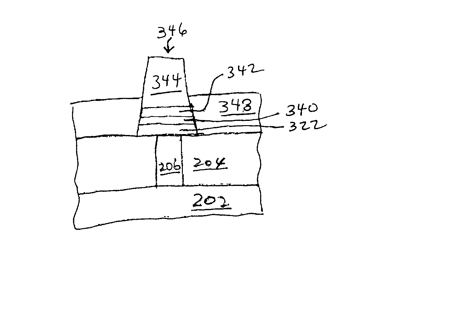
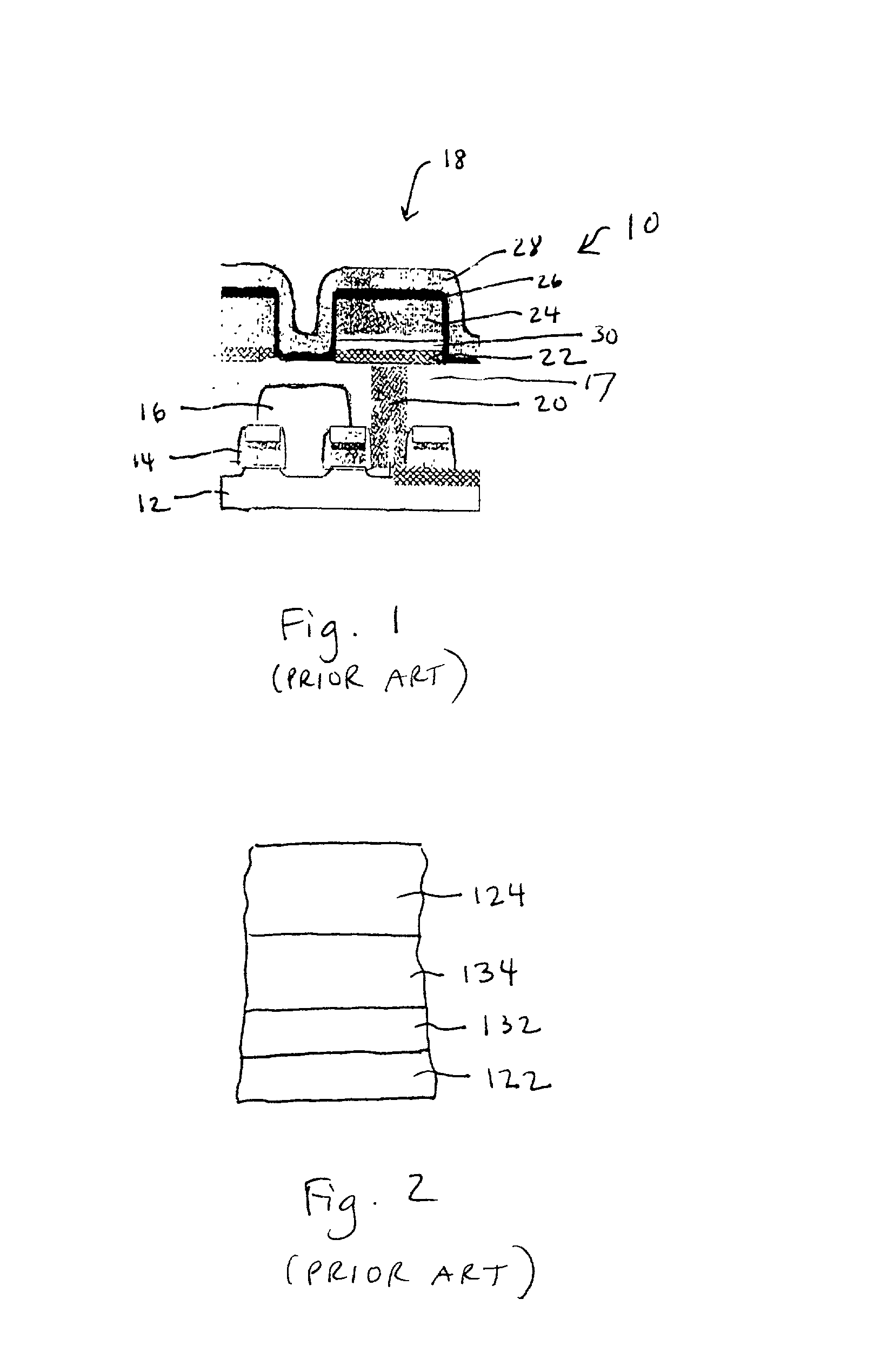
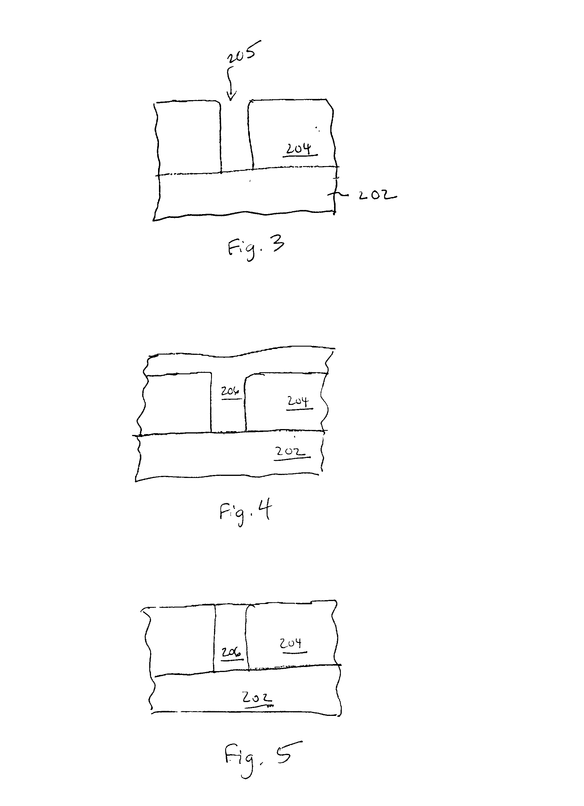
[0024] A description of preferred embodiments of the present invention will be discussed, followed by a comparison of prior art electrode molecular grain structures with the present invention molecular structure, and a discussion of some advantages of the invention. Only one electrode is shown in each figure, although many electrodes and other components of a memory cell are present in the semiconductor devices shown.
[0025] FIGS. 3-14 show two preferred embodiments of the present multi-layer memory electrode invention in various stages of fabrication. FIG. 3 shows a cross-sectional view of a semiconductor memory device having a workpiece 202. Workpiece 202 preferably comprises a semiconductor substrate such as silicon. Alternatively, other circuit components may reside within workpiece 202, although the top surface of the workpiece 202 preferably comprises an oxide such as silicon dioxide, for example. In accordance with the present invention, an insulating layer 204 is deposited ov...
PUM
 Abstract
Description
Claims
Application Information