Light emitting device

a technology of light emitting device and light source, which is applied in the direction of solid-state devices, electric lighting sources, electric light sources, etc., can solve the problems of affecting the efficiency of light emission, affecting the effect of driver voltage reduction, and difficult noise development,

Inactive Publication Date: 2002-08-08
SEMICON ENERGY LAB CO LTD
View PDF65 Cites 92 Cited by
  • Summary
  • Abstract
  • Description
  • Claims
  • Application Information

AI Technical Summary

Problems solved by technology

In addition, drive using a direct current voltage is possible because the organic light emitting elements are light emitting elements of a carrier injecting type, and therefore it is difficult for noise to develop.
For example, if the organic light emitting elements have only a single layer of Alq.sub.3, then almost all electrons injected from the cathode will reach the anode without recombining with holes because Alq.sub.3 has electron transporting properties, and the efficiency of light emission is extremely bad.
First, one problem is hindrance of an additional reduction in a driver voltage.
In addition, another problem originates in an organic interface is exertion of influence on the element lifetime (element deterioration) for organic light emitting elements.
Namely, brightness drops because the carrier mobility is impeded and charge accumulates.
However, carrier mobility is suppressed due to the formation of organic interfaces, in particular interfaces which block carriers, and this in turn influences the reductions in the driver voltage and in brightness.
In particular, the conformity of junction in the organic interface is thought to become worse for cases in which a heterostructure is formed using materials having large differences in their molecular size.
Furthermore, carriers unable to overcome the energy barrier accumulate as a charge, and there is a possibility that this will cause a drop in brightness as disc

Method used


Image

  • Light emitting device
  • Light emitting device
  • Light emitting device

Examples


embodiments

Embodiment 1

[0119] A specific example of an organic light emitting element in which a hole injecting region made from a hole injecting material is inserted between the anode 402 and the organic compound film 403 is shown in this embodiment for the organic light emitting elements of FIG. 7A.

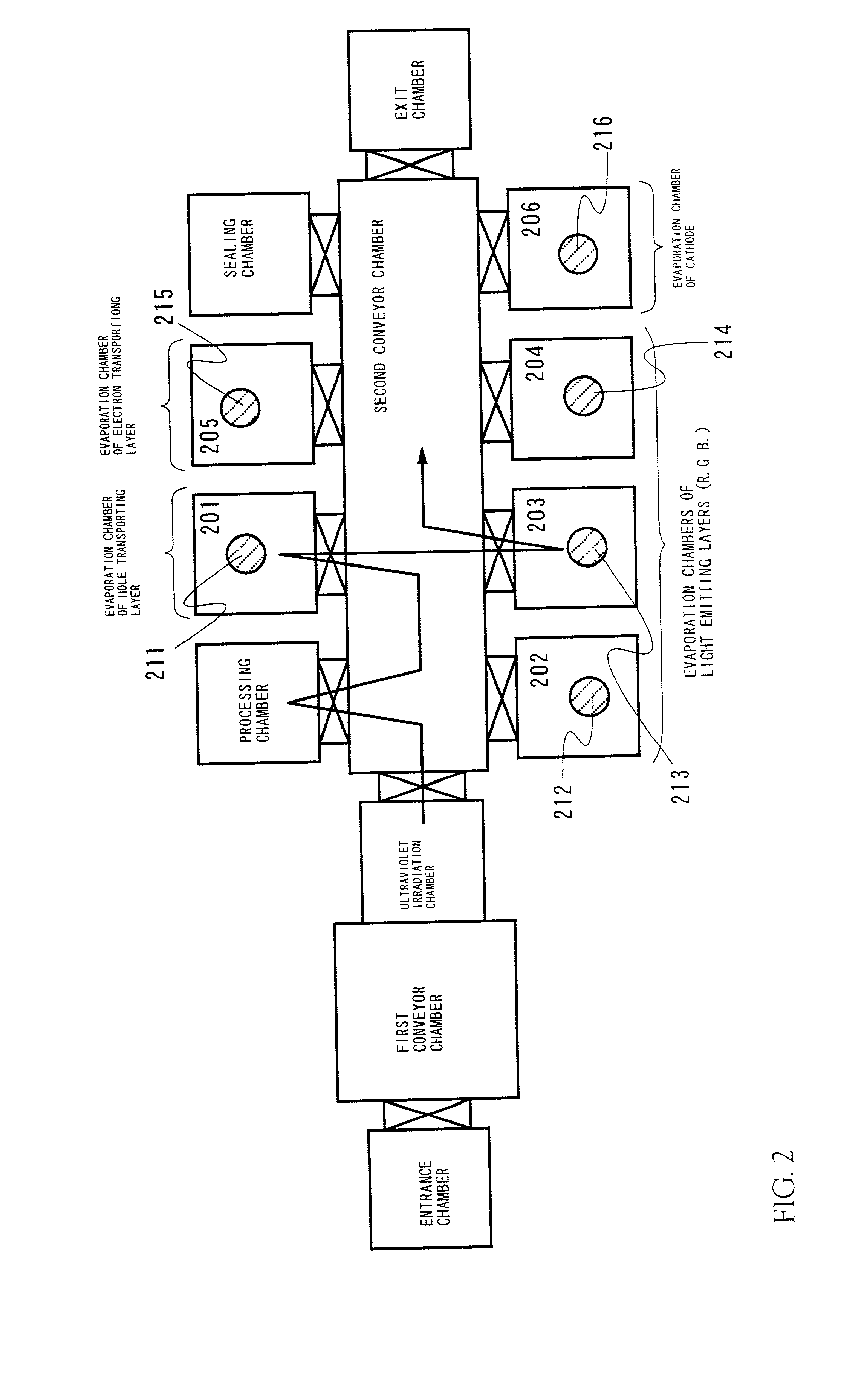
[0120] First, the glass substrate 401 on which a film is formed from ITO by sputtering to a thickness on the order of 100 nm and the anode 402 is formed is prepared. The glass substrate 401 having the anode 402 is then conveyed to the inside of a vacuum chamber like that shown in FIGS. 9A and 9B. Five evaporation sources are necessary in this embodiment in order to evaporate five types of materials (four of the materials are organic compounds, and one is a metal that becomes a cathode).

[0121] The hole injecting material CuPc is evaporated for 20 nm first, and when the 20 nm thickness of CuPc evaporation is completed, evaporation of the hole transporting material .alpha.-NPD at an evaporation rate ...

embodiment 2

[0126] A specific example of the organic light emitting element shown in FIG. 8B is shown in this embodiment.

[0127] First, the glass substrate 401 on which a film is formed from ITO by sputtering to a thickness on the order of 100 nm and the anode 402 is formed is prepared. The glass substrate 401 having the anode 402 is then conveyed to the inside of a vacuum chamber like that shown in FIGS. 9A and 9B. Five evaporation sources are necessary in this embodiment in order to evaporate five types of materials (four of the materials are organic compounds, and one is a metal that becomes a cathode).

[0128] After forming the hole transporting region 405 to a thickness of 30 nm only from the hole transporting material MTDATA (evaporation rate of 3 .ANG. / sec), the shutter to the MTDATA evaporation source is gradually closed, while the shutter to an evaporation source of the electron transporting material PBD is gradually opened. The first concentration change region 406 with a thickness on th...

embodiment 3

[0132] A specific example in which a hole injecting region made from a hole injecting material is inserted between the anode 402 and the organic compound film 403, an electron injecting region made from an electron injecting material is respectively inserted between the cathode 404 and the organic compound film 403, and a triplet light emitting material is applied as the light emitting material in the organic light emitting element is discussed in this embodiment. The element structure is shown in FIG. 10.

[0133] First, the glass substrate 1000 on which a film is formed from ITO by sputtering to a thickness on the order of 100 nm and the an ITO is formed is prepared. The glass substrate having the ITO is then conveyed to the inside of a vacuum chamber like that shown in FIGS. 9A and 9B. Seven evaporation sources are necessary in this embodiment in order to evaporate seven types of materials (five of the materials are organic compounds, and two are inorganic compounds that become cath...


PUM


Abstract

A light emitting device and electronic equipment having a long life at a low electric power consumption are provided. A hole transporting region composed of a hole transporting material, an electron transporting region composed of an electron transporting material, and a mixture region in which both the hole transporting material and the electron transporting material are mixed at a fixed ratio are formed within an organic compound film. Regions having a concentration gradient are formed between the mixture region and carrier transporting regions until the fixed ratio is achieved. In addition, by doping a light emitting material into the mixture region, functions of hole transportation, electron transportation, and light emission can be respectively expressed while all of the interfaces existing between layers of a conventional lamination structure are removed. Organic light emitting elements having low electric power consumption and a long life can thus be provided, and light emitting devices and electronic equipment can be manufactured using the organic light emitting elements.

Description

[0001] 1. Field of the Invention[0002] The present invention relates to a light emitting device using an organic light emitting element having an anode, a cathode, and a film containing an organic compound in which light emission can be obtained by applying an electric field (hereafter referred to as an "organic compound film"). In particular, the present invention relates to a light emitting device using organic light emitting elements having a driver voltage that is lower than a conventional driver voltage and having a long life. Note that the term light emitting device within this specification indicates image display devices or light emitting devices using organic light emitting elements as light emitting elements. Further, modules in which a connector, for example, an anisotropic conductive film (flexible printed circuit, FPC), a TAB (tape automated bonding) tape, or a TCP (tape carrier package) is attached to organic light emitting elements, modules in which a printed-wiring b...

Claims


Application Information

Patent Timeline
IPC IPC(8): H01L27/32H01L51/50H01L51/00H01L51/30H05B33/14H05B33/22
CPCH01L27/32H01L51/005H01L51/0059H01L51/0081H01L51/5008H01L51/5012H10K59/00H10K85/60H10K85/631H10K85/324H10K30/865H10K50/11H05B33/14
Inventor SEO, SATOSHIYAMAZAKI, SHUNPEI
Owner SEMICON ENERGY LAB CO LTD
Why Eureka
Try Eureka