

Semiconductor device and manufacturing method thereof
a technology of semiconductor devices and semiconductors, applied in semiconductor devices, semiconductor/solid-state device details, capacitors, etc., can solve the problems of increasing the number of interconnection layers formed on the interlayer insulating film, the structure of the above pad is not easy to achieve, and the processing accuracy of the interconnection layer is difficult to ensur
- Summary
- Abstract
- Description
- Claims
- Application Information
AI Technical Summary
Problems solved by technology
Method used
Image

Examples
second embodiment
[0087] Second Embodiment
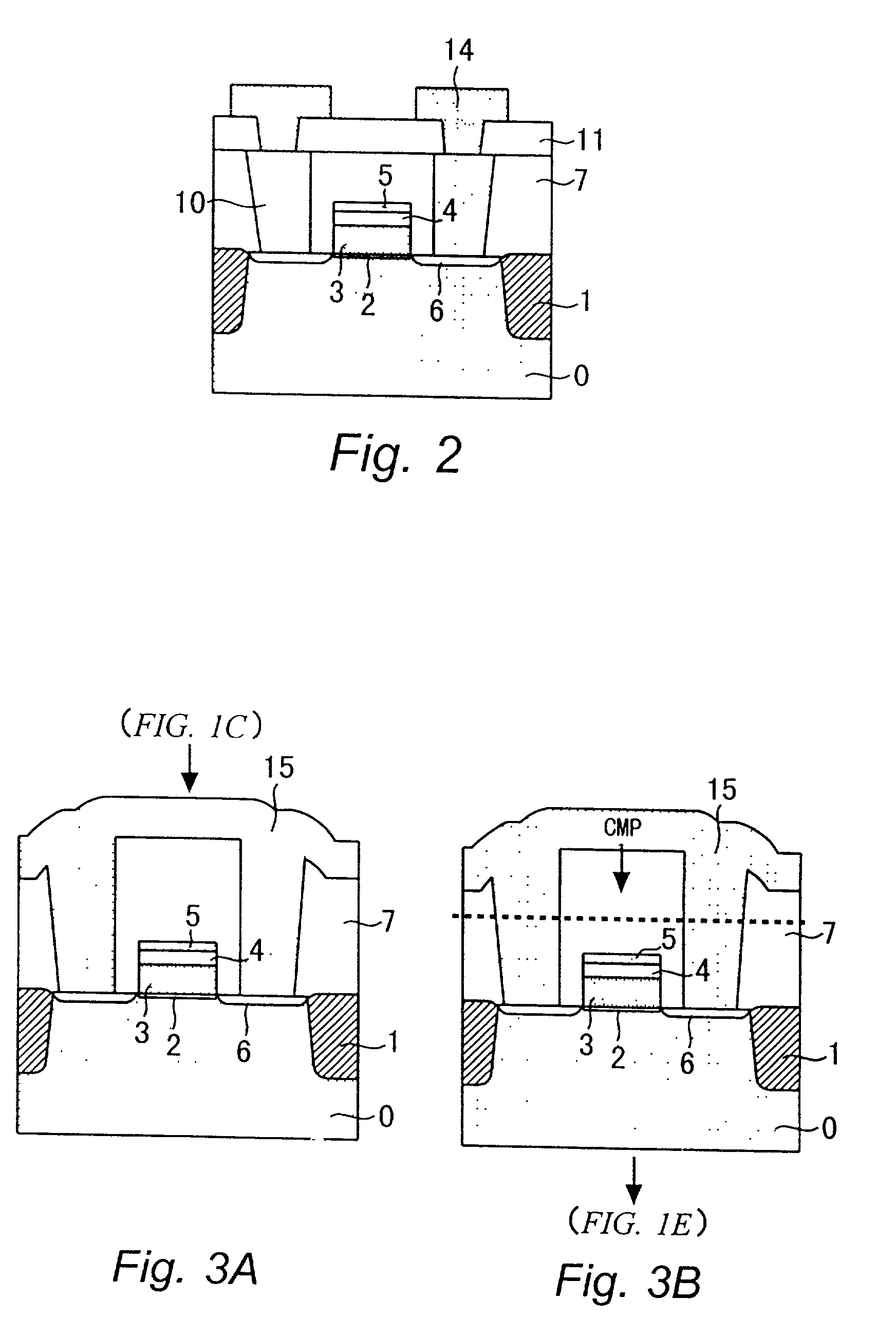
[0088] A second embodiment of the present invention will be described with reference to FIGS. 3A and 3B. FIGS. 3A and 3B are cross-sectional views illustrating essential part of a method of manufacturing a semiconductor device according to the second embodiment.
[0089] According to the manufacturing method in the first embodiment, doped silicon for forming the pads 10 is deposited over the entire surface of the silicon substrate 0 and the entire surface of the silicon substrate 0 is etched back by dry etching. Such a state is shown in FIG. 1D. Then, the unnecessary portion of the silicon oxide film 7 is removed by CMP, to planarize the surfaces of the pads 10 and the surface of the silicon oxide film 7 at the same level.
[0090] On the contrary, according to the manufacturing method in the second embodiment, as shown in FIG. 3A, after deposition of doped silicon 15 over the entire surface of the silicon substrate 0, CMP is performed without carrying out etching ...
fourth embodiment
[0100] Fourth Embodiment
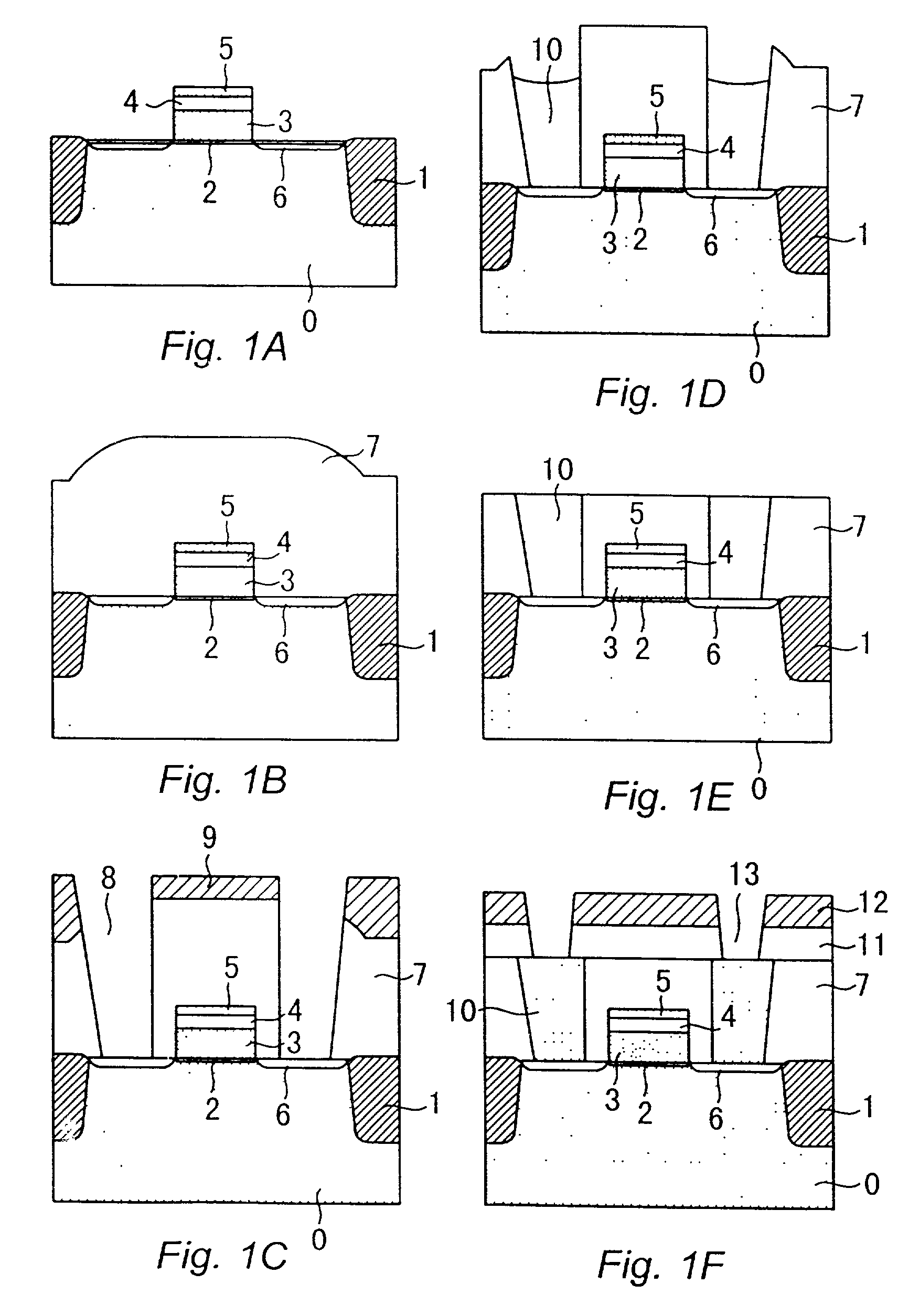
[0101] A fourth embodiment of the present invention will be described with reference to FIGS. 5A to 5E. FIGS. 5A to 5E are cross-sectional views illustrating essential part of a method of a semiconductor device according to the fourth embodiment.
[0102] According to the manufacturing method in the fourth embodiment, contact holes 13 opened to pads 10 are formed in the same manner as that in the first embodiment (see FIG. 1F). After formation of the contact holes 13, as shown in FIG. 5A, a first high melting point metal film 19 is formed in such a manner as to cover the inner walls of the contact holes 13, the exposed portions of the pads 19, and the surface of the silicon oxide film 11. The first high melting point metal film 19 is formed in the same manner as that for forming the high melting point metal film 16 in the third embodiment.
[0103] Referring to FIG. 5B, the wafer is subjected to RTA, to produce a silicide film 20 near the boundary between the first...
fifth embodiment
[0112] Fifth Embodiment
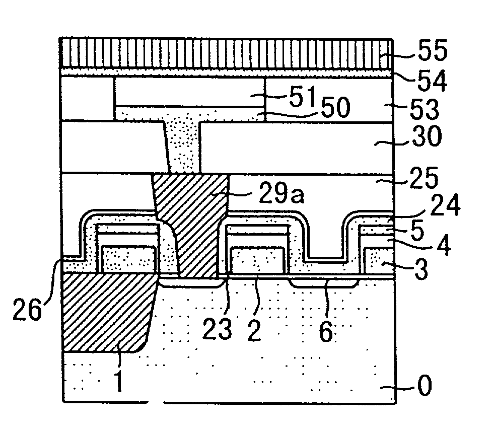
[0113] A fifth embodiment of the present invention will be described with reference to FIGS. 6A to 6F and FIGS. 7A to 7C. FIGS. 6A to 6F and FIGS. 7A to 7C are cross-sectional views illustrating a structure of a semiconductor device and a manufacturing method thereof according to the fifth embodiment. In the semiconductor device in the fifth embodiment, a capacitor portion of a DRAM has the same structure as that in the first embodiment.
[0114] According to the manufacturing method in this embodiment, as shown in FIG. 6A, a transistor is formed on a silicon substrate 0 in the same manner as that in the first embodiment.
[0115] Referring to FIG. 6B, the silicon substrate 0 is subjected to oxidation treatment to form a silicon oxide film 23 on the side surfaces of a gate silicon film 3. Then, a silicon nitride film 24 is deposited over the entire surface of the substrate 0. To desirably keep a hot carrier characteristic of the transistor, it is required to avoid d...
PUM
| Property | Measurement | Unit |
|---|---|---|
| temperature | aaaaa | aaaaa |
| aspect ratio | aaaaa | aaaaa |
| temperature | aaaaa | aaaaa |
Abstract
Description
Claims
Application Information