Thin film semiconductor device, polycrystalline semiconductor thin film production process and production apparatus

a thin film semiconductor and production process technology, applied in the direction of crystal growth process, wing accessories, manufacturing tools, etc., can solve the problems of inability to grow polycrystalline silicon having a large grain size or control the grain size, difficult to improve the characteristic properties, reliability and uniformity of tft devices, and the grain size of polycrystalline silicon 103 is 0.5 .mu.m or less

Inactive Publication Date: 2002-08-29
PANASONIC LIQUID CRYSTAL DISPLAY CO LTD +1
View PDF0 Cites 100 Cited by
  • Summary
  • Abstract
  • Description
  • Claims
  • Application Information

AI Technical Summary

Benefits of technology

[0009] It is a second object of the present invention to provide a production process and apparatus for forming a low-cost and high-quality polycrystalline semiconductor film, which can reduce the number of production steps, can be applied to a large-area substrate and have a high throughput, and to provide a thin film semiconductor device comprising the above polycrystalline semiconductor film.
[0010] It is a third object of the present invention to provide a production process and apparatus for forming on an inexpensive insulating substrate made from glass or the like a high-quality polycrystalline semiconductor film which operates with high performance and high reliability and is excellent in uniformity among devices, and to provide a thin film semiconductor device comprising the above polycrystalline semiconductor film.
[0014] It is possible to provide a thin film semiconductor device having high reliability by selecting the main orientation of the semiconductor film of the channel region with respect to the main surface of the insulating substrate or the gate insulating film even when a polycrystalline semiconductor film is used. The method of controlling the main orientation of the polycrystalline film will be described hereinafter.
[0024] The third aspect of the present invention is more preferred. That is, the channel region of the first semiconductor film is composed of crystal grains having such a length in a longitudinal direction as to connect the first charge transmitting and receiving means and the second charge transmitting and receiving means. Therefore, a thin film semiconductor device having higher reliability can be provided.
[0026] the main orientation of the first semiconductor film constituting the channel region is {110} with respect to the main surface of the insulating substrate or the gate insulating film; and the main orientation of the surface of the first semiconductor film substantially perpendicular to a direction for connecting the first and second charge transmitting and receiving means is {100}. The channel region of the first semiconductor film is composed of crystal grains having a length in a longitudinal direction for connecting the first charge transmitting and receiving means and the second charge transmitting and receiving means, and the main orientation of the polycrystalline film is {100}, thereby making it possible to provide a thin film semiconductor device having extremely high reliability. Briefly speaking the conclusion, this is because each crystal grain has the same properties as a monocrystal though the first semiconductor film is polycrystal.

Problems solved by technology

Therefore, the obtained polycrystalline silicon film 103 has a grain size of 0.5 .mu.m or less and is not uniform in size.
Therefore, it is impossible to grow polycrystalline silicon having a large grain size or to control the grain size or the position of the grain boundary accurately.
Consequently, it is difficult to improve the characteristic properties, reliability and uniformity of TFT devices.
Since the beam must be converged to a size of 1 .mu.m or less in the technology disclosed by the above international patent publication WO9745827, the energy of the laser is lost and the optical system of an irradiation laser become complicated.
As the moving distance between laser pulses is 1 .mu.m or less, it takes a long time to crystallize the whole substrate and it is difficult to improve throughput and reduce costs.
Particularly, this process cannot be applied to a large-area substrate.
Further, very small distance movement is easily influenced by vibration and involves a yield problem.

Method used


Image

  • Thin film semiconductor device, polycrystalline semiconductor thin film production process and production apparatus
  • Thin film semiconductor device, polycrystalline semiconductor thin film production process and production apparatus
  • Thin film semiconductor device, polycrystalline semiconductor thin film production process and production apparatus

Examples


embodiment 1

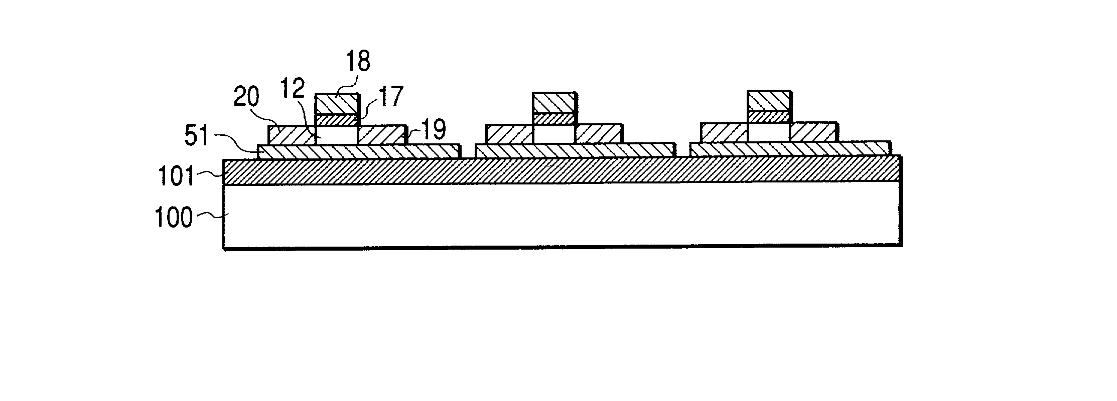
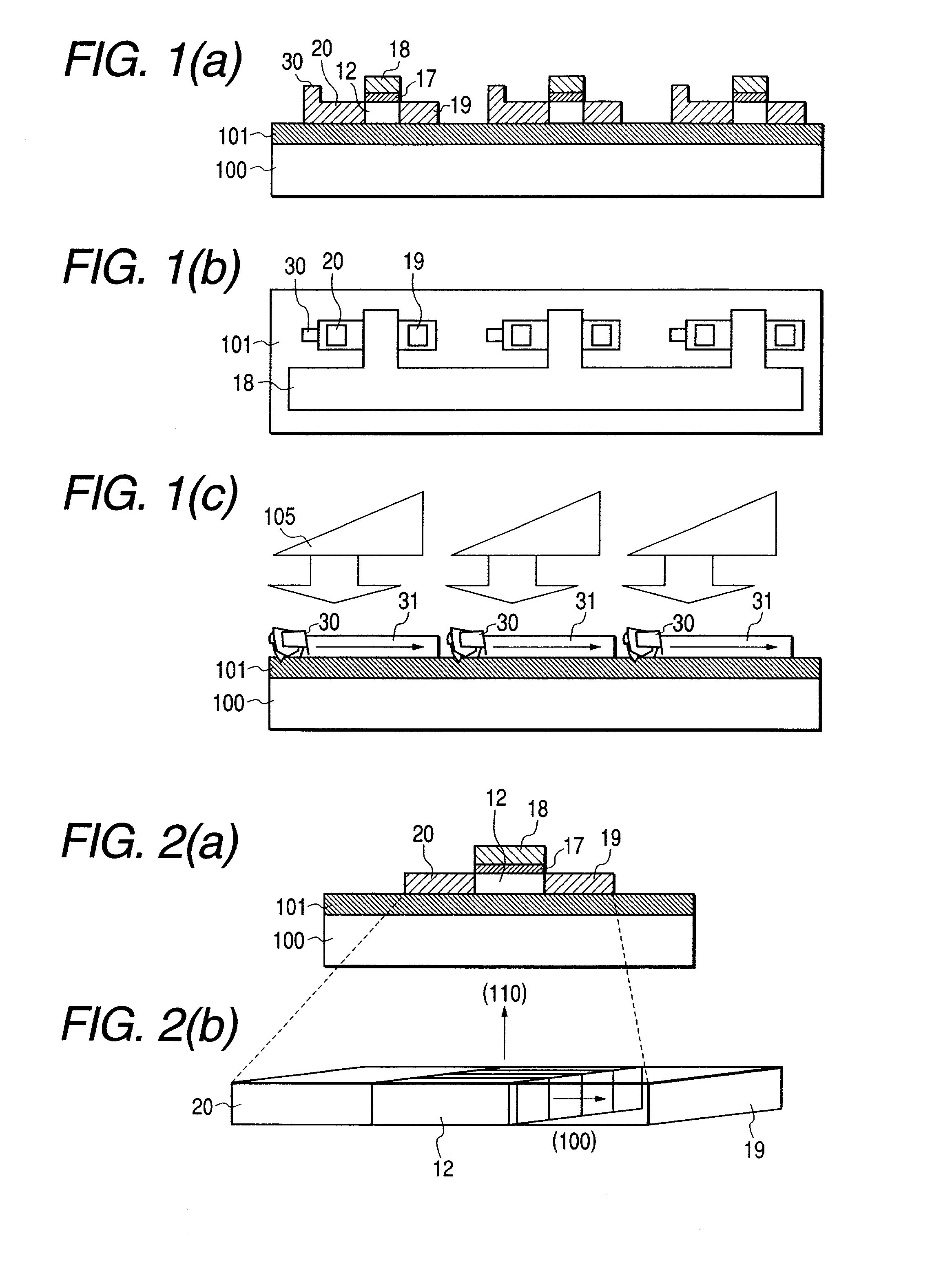
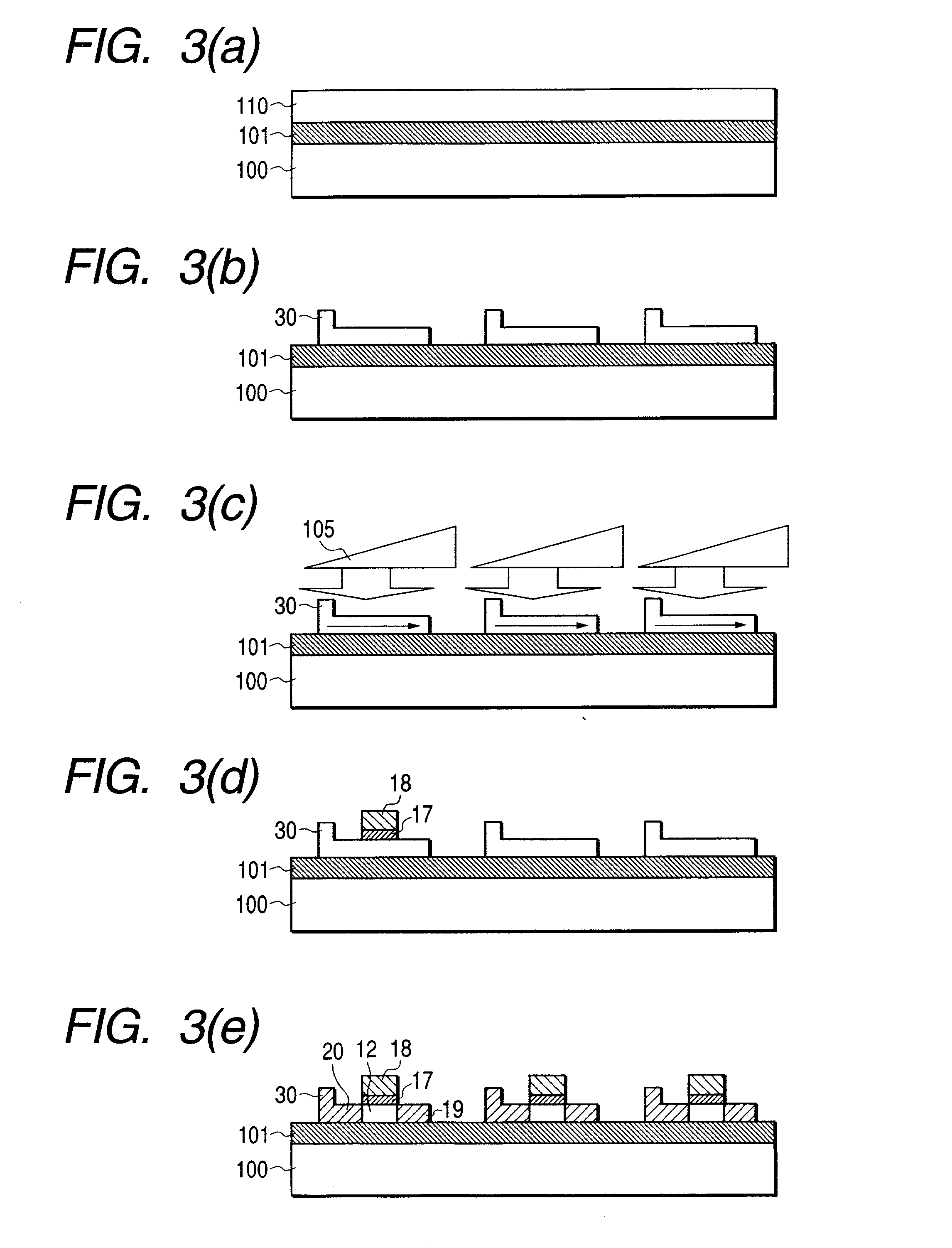
[0077] FIGS. 1(a) to 1(c) are diagrams for explaining a thin film semiconductor device of the present invention. FIGS. 1(a) to 1(c) show the thin film semiconductor device having three polycrystalline silicon thin film transistors. FIG. 1(a) is a sectional view and FIG. 1(b) is a plan view of the thin film semiconductor device. In FIG. 1(a) and FIG. 1(b), reference numeral 100 denotes an insulating substrate, 101 underlying layer film, 18 gate electrode and 17 gate insulating film. A glass substrate is frequently used as the insulating substrate. A silicon dioxide (SiO.sub.2) film is generally used as the above underlying layer film.

[0078] Each silicon semiconductor layer comprises a channel region 12, a source region 20, a drain region 19 and a projecting crystal nucleus region 30. The channel region 12 is composed of a polycrystalline silicon film having a large grain size and the crystal nucleus region 30 is generally composed of a polycrystalline silicon film having a small gra...

embodiment 2

[0095] FIGS. 7(a) to 7(c) are diagrams for explaining a semiconductor device of the present invention. In this embodiment, a second semiconductor layer is formed below the semiconductor layer constituting a channel from the viewpoint of crystal growth. FIGS. 7(a) to 7(c) show three polycrystalline silicon thin film transistors mounted. FIG. 7(a) is a sectional view and FIG. 7(b) is a plan view of the semiconductor device. FIG. 7(c) is a sectional view for explaining a laser beam irradiation method.

[0096] In FIG. 7(a) and FIG. 7(b), reference numeral 100 denotes an insulating substrate, 101 underlying layer film, 18 gate electrode and 17 gate insulating film. A glass substrate is frequently used as the insulating substrate. A silicon dioxide film is generally used as the underlying layer film.

[0097] The first semiconductor layer has a channel region 12, source region 20 and drain region 19. The channel region 12 is composed of a polycrystalline silicon film having a large grain size...

embodiment 3

[0105] FIGS. 9(a) to 9(c) are diagrams for explaining a semiconductor device of the present invention. In this embodiment, a member which facilitates the partial radiation of heat during crystal growth is used.

[0106] FIGS. 9(a) to 9(c) show a semiconductor device having three polycrystalline silicon thin film transistors formed thereon. FIG. 9(a) is a sectional view and FIG. 9(b) is a plan view of the semiconductor device.

[0107] In FIGS. 9(a) and 9(b), reference numeral 100 denotes an insulating substrate, 101 underlying layer film, 19 gate electrode and 17 gate insulating film. The semiconductor layer is composed of a channel region 12, source region 20 and drain region 19, and the channel region 12 is composed of a polycrystalline silicon film having a large grain size. An insulating film 50 is selectively formed on the underlying layer film 101 between a plurality of semiconductor devices. The heat conductivity of the insulating film 50 is higher than the heat conductivity of th...


PUM

PropertyMeasurementUnit
lengthaaaaaaaaaa
widthaaaaaaaaaa
internal tensile stressaaaaaaaaaa

Abstract

In an MIS field effect transistor having a gate electrode formed on a first semiconductor layer which is a polycrystalline silicon film on an insulating substrate through a gate insulating film, a channel region formed in the semiconductor layer and a source region and a drain region arranged on both sides of the channel region, a thin film semiconductor device has a main orientation of at least the channel region of {110} with respect to the surface of the gate insulating film. Further, a polycrystalline semiconductor film having a main orientation of the surface almost perpendicular to a direction for connecting the source and drain regions of {100} is preferably used in the channel of a semiconductor device. According to the present invention, a semiconductor device having a high-quality polycrystalline semiconductor film whose grain boundary, grain size and crystal orientation can be controlled and whose film roughness and crystal defects formed by crystallization have been reduced can be obtained on the insulating substrate.

Description

[0001] 1. Field of the Invention[0002] The present invention relates to a thin film semiconductor device having a polycrystalline semiconductor film, and a process and apparatus for producing a polycrystalline semiconductor film. The thin film semiconductor device of the present invention is useful for image display devices.[0003] 2. Related Art[0004] The prior art process for crystallizing an amorphous silicon thin film by scanning with a pulse laser will be described with reference to FIG. 12. FIG. 12 shows the most general process for crystallizing with an excimer pulse laser of the prior art. The whole substrate is crystallized by irradiating a non-crystal silicon film 102 which was formed on a substrate 100 through an base film 101, with a laser beam 105 from a linear excimer laser having a width L of several millimeters on the substrate and moving the laser exposure position at intervals of 1 to several pulses. In this prior art process, crystal nuclei are formed at random upo...

Claims


Application Information

Patent Timeline
Patent Type & Authority Applications(United States)
IPC IPC(8): H01L29/786C30B1/00H01L21/00H01L21/20H01L21/26H01L21/324H01L21/336H01L21/36H01L21/42H01L21/44H01L21/4763H01L21/477H01L21/84H01L23/62H01L27/01H01L27/12H01L31/0328H01L31/0336H01L31/0392H01L31/072H01L31/109
CPCB23K26/063H01L21/02686H01L21/02691H01L27/1281H01L27/1285H01L27/1296H01L29/04H01L29/78675B23K26/0622E05C17/446E05Y2201/47E05Y2900/132
Inventor HATANO, MUTSUKOYAMAGUCHI, SHINYAKIMURA, YOSHINOBUPARK, SEONG-KEE
Owner PANASONIC LIQUID CRYSTAL DISPLAY CO LTD
Why Eureka
Try Eureka