These requirements place significant limitations on the materials and thicknesses of the transparent
cathode.
However, even though such a relatively low resistivity may be acceptable for certain types of applications, such a resistivity may still be somewhat too high for a passive
matrix array of
OLED pixels in which the current that powers each pixel needs to be conducted across the entire array through the narrow strips of the compound
cathode.
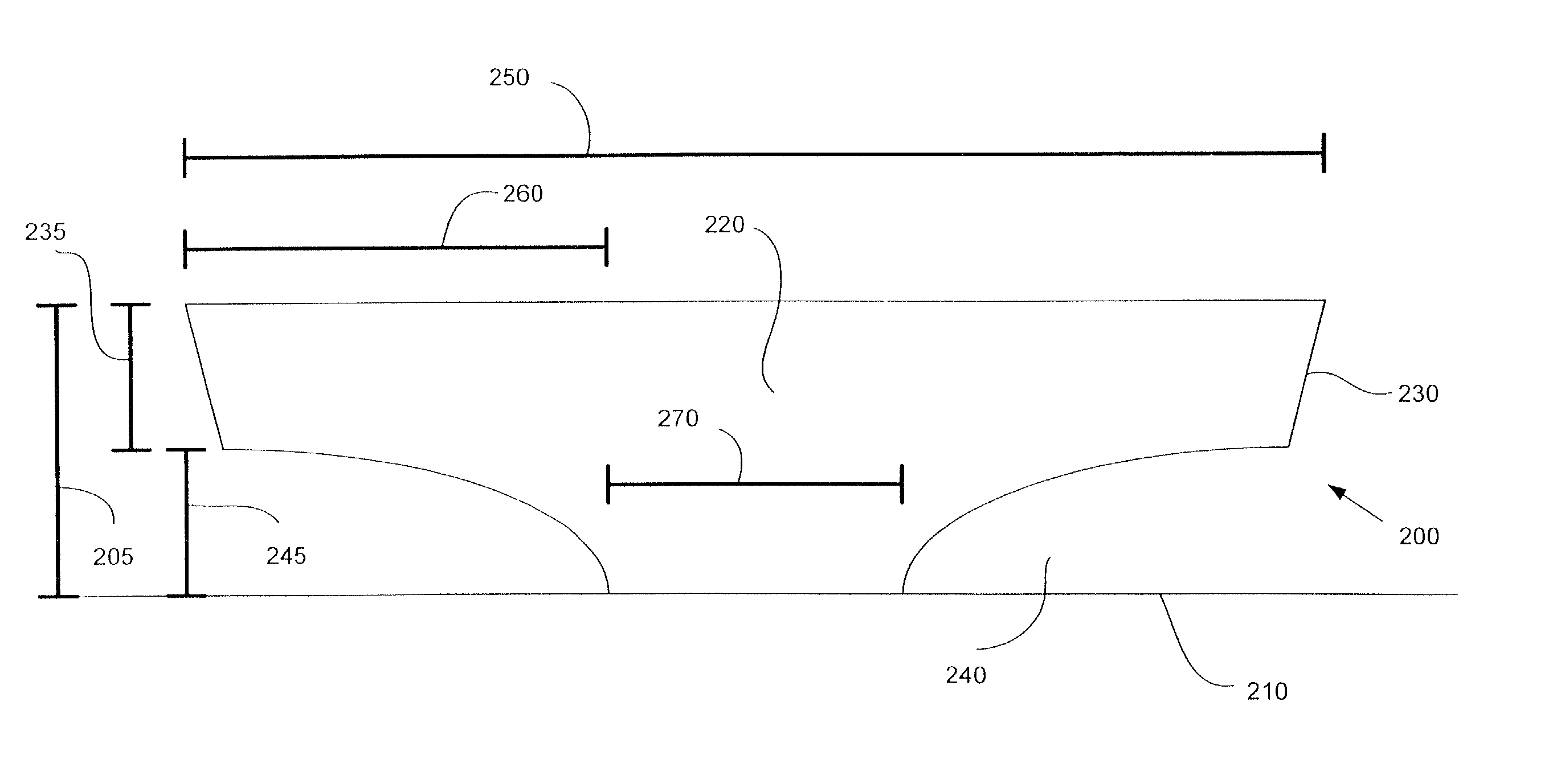
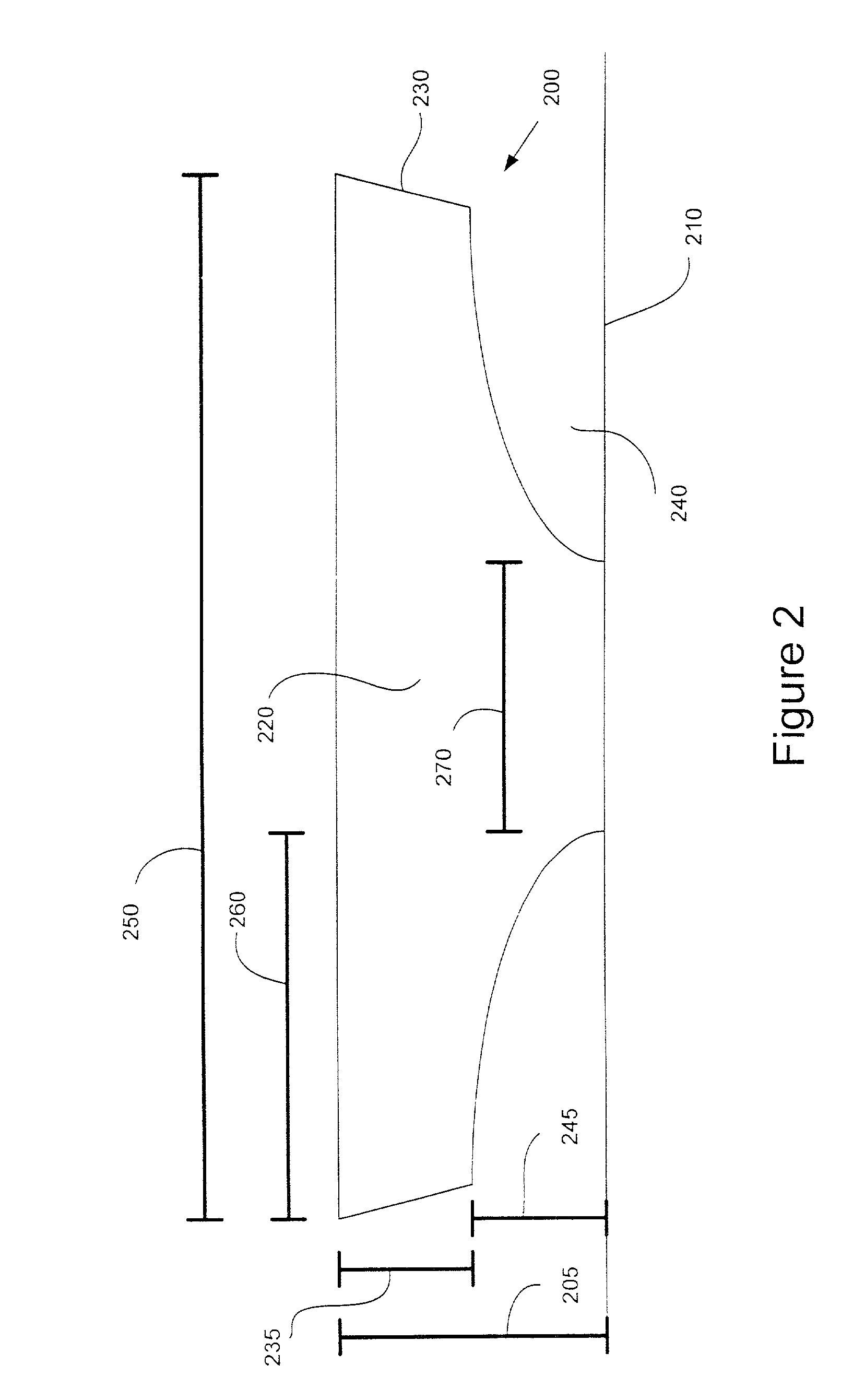
Because the
bus line is made of a thick
electrically conductive material, it does not transmit light, and unfavorably results in an inactive area on the array of OLEDs.
For example, any
exposure to high temperature or chemical
processing may damage the organic
layers and adversely affect device reliability.
As a result, the processes conventionally used to fabricate a thick
metal feature such as a
bus line may damage any organic
layers that are already present.
Using an integrated mask is particularly desirable where the steps used to pattern material or to remove a mask have the potential to damage the device.
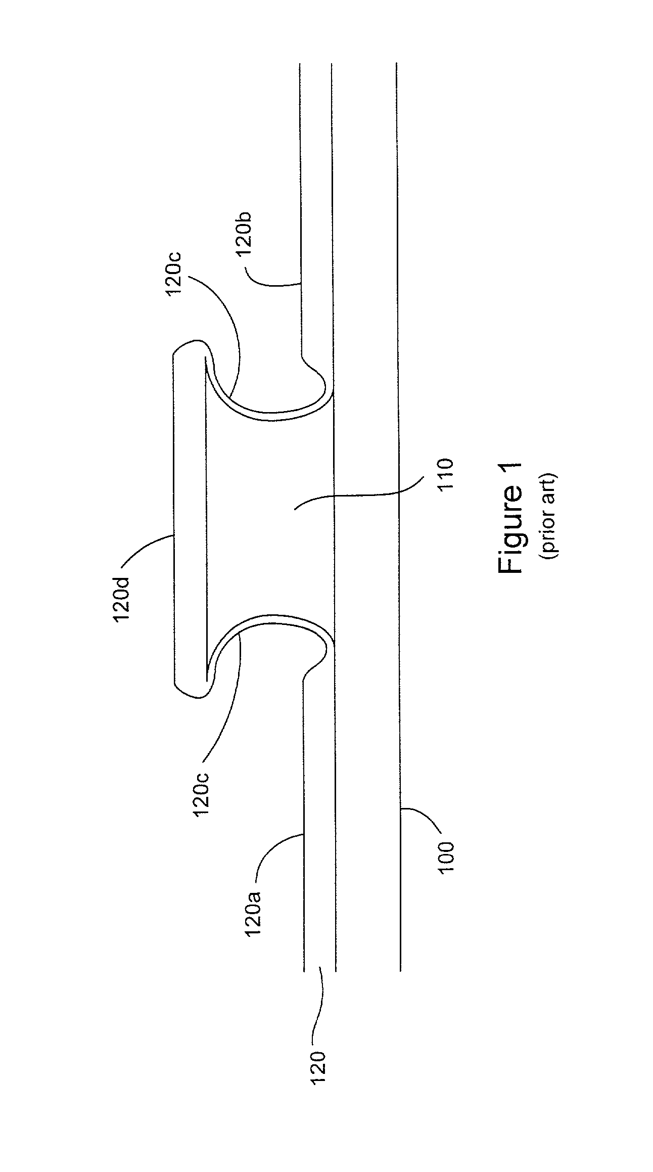
One problem that has been observed with conventional integrated masks is the shorting of adjacent
electrode layers across the mask.
First, in order to avoid shorting problems, the "
footprint" of the deposited material, defined as the surface area onto which significant material is deposited, should be sharply limited to those surfaces having a direct
line of sight, unobstructed by the mask, to the source of material being deposited. The
footprint should not extend onto surfaces that do not have a direct
line of sight to the source of deposited material. Whether deposition is limited in this way is dependent upon the
deposition process. Processes such as low energy deposition of metals by thermal
evaporation, generally result in
footprint relatively sharply limited to surfaces having a direct
line of sight to the source of material. In contrast, processes such as
chemical vapor deposition may result in a significantly larger footprint, such that there is significant deposition onto surfaces not having a direct line of
sight to the source of material. Processes such as sputter depositing have a footprint between that of thermal
evaporation and that of
chemical vapor deposition. One mechanism that may lead to a larger footprint is collisions between atoms or molecules of the material being deposited during transit to the substrate, and the
resultant scattering. A low "sticking efficiency" of the atoms or molecules being deposited is another such mechanism. These mechanisms may lead to the side walls of a conventional integrated mask being coated with substantial quantities of the material being deposited even though such surfaces may not be within a direct line of
sight from the
source material.
Second, in order to avoid shorting problems, deposition that is significantly off-axis should be avoided, even for processes that have a limited footprint. Off-axis deposition is deposition from an angle not perpendicular to the substrate. Off-axis deposition may result in surfaces losing their protection from a direct line of
sight to the source of material being deposited, such that material may be deposited into the recessed area under an overhang. Moreover, off-axis deposition often involves deposition from a variety of different angles, such that even more surface area loses protection from a direct line of sight during the process. Off-axis deposition may occur for many reasons. For example, the geometry of the substrate, the source, and their relative locations may lead to significant off-axis deposition, and may even lead to significant variations in the angle of deposition at different points on the substrate. The substrate may be placed on a moving
conveyor belt during deposition, which inherently leads to off-axis deposition when the substrate is not directly beneath the source of material, and may lead to very large angle off-axis deposition when the substrate is at the edge of the
deposition chamber. The substrate may also be rotated during deposition. Even processes that have a somewhat limited footprint, such as sputter depositing, may lead to shorting if there is significant off-axis deposition. It is believed that sputter depositing through a conventional integrated mask leads to shorting when off-axis deposition from angles of about 30 degrees or greater is present, although there may be shorting at smaller angles depending upon the exact process parameters.
However, such processes may cause deposition to occur in undesirable regions of the device.
Thus, using conventional integrated masks, it may not be possible to fabricate desirable but previously unattainable structures such as transparent or top-emitting OLEDs using a compound Mg:Ag / ITO
cathode in a passive matrix OLED array.
The use of such a conventional mask may result in the ITO layer causing harmful shorting across adjacent compound cathode strips.
However, if the vapor
deposition process produces too much scattering and is, thus, insufficiently unidirectional, residual layer 120c may be continuous and have significant electrical
conductivity.

