Method of forming a multilayer dielectric stack

a technology of dielectric stack and multilayer layer, which is applied in the manufacture of semiconductor devices, nanostructures, electrical apparatus, etc., can solve the problems of non-uniform electrical fields, very rough surface of film, and development of crystalline structures under normal integrated circuit manufacturing conditions, so as to reduce or eliminate the formation of crystalline structures, reduce the tunneling current, and improve device performance

Inactive Publication Date: 2002-09-19
SHARP LAB OF AMERICA INC
View PDF0 Cites 57 Cited by
  • Summary
  • Abstract
  • Description
  • Claims
  • Application Information

AI Technical Summary

Benefits of technology

0009] Preferably, alternating layers of high-k material and interposing material replace prior art silicon dioxide dielectric layers in integrated circuits. Each layer is preferably between less than 50 angstroms thick. The thin layers of high-k material bounded by interposing material reduces or eliminates the formation of crystalline structures. The multiple layers reduce the tunneling current, which allows ...

Problems solved by technology

One common problem associated with the above-mentioned high-k dielectrics is that they develop a crystalline structure under normal integrated circuit manufacturing conditions.
As a result, the surface of the film is very rough.
Surface roughness causes non-uniform electrical fields in the channel region adjacent the dielectric film.
Such films are not suitable for the gate dielectrics of ...

Method used


Image

  • Method of forming a multilayer dielectric stack
  • Method of forming a multilayer dielectric stack
  • Method of forming a multilayer dielectric stack

Examples


Embodiment Construction

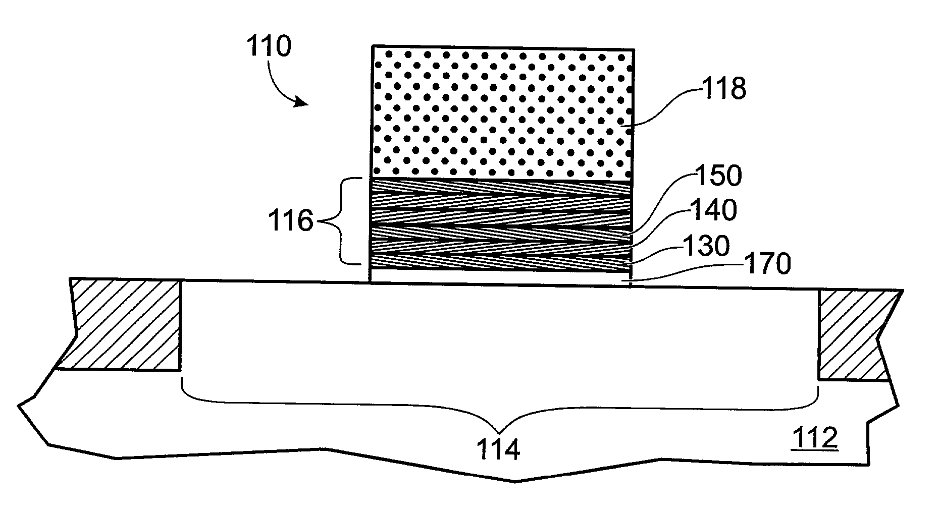
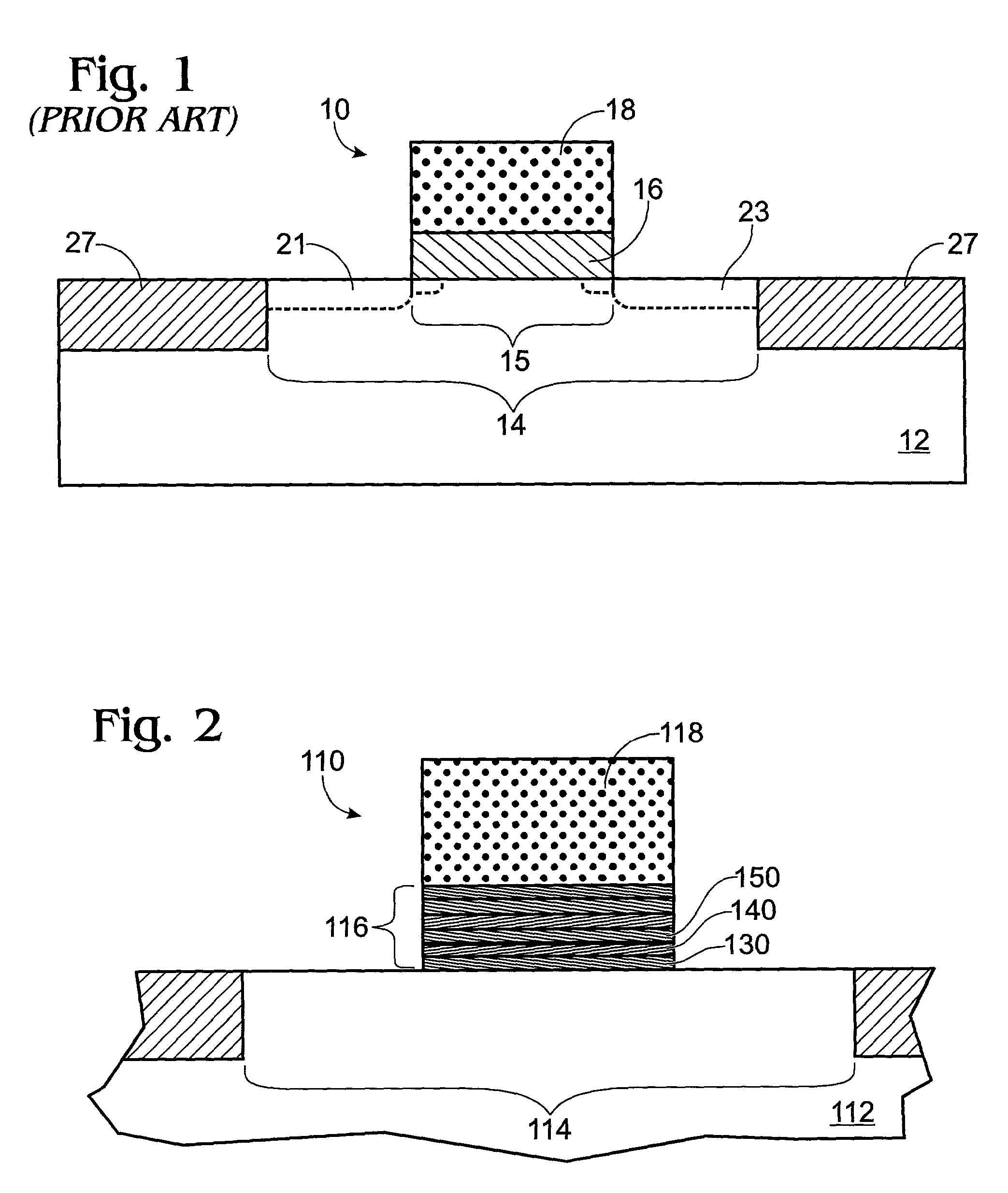
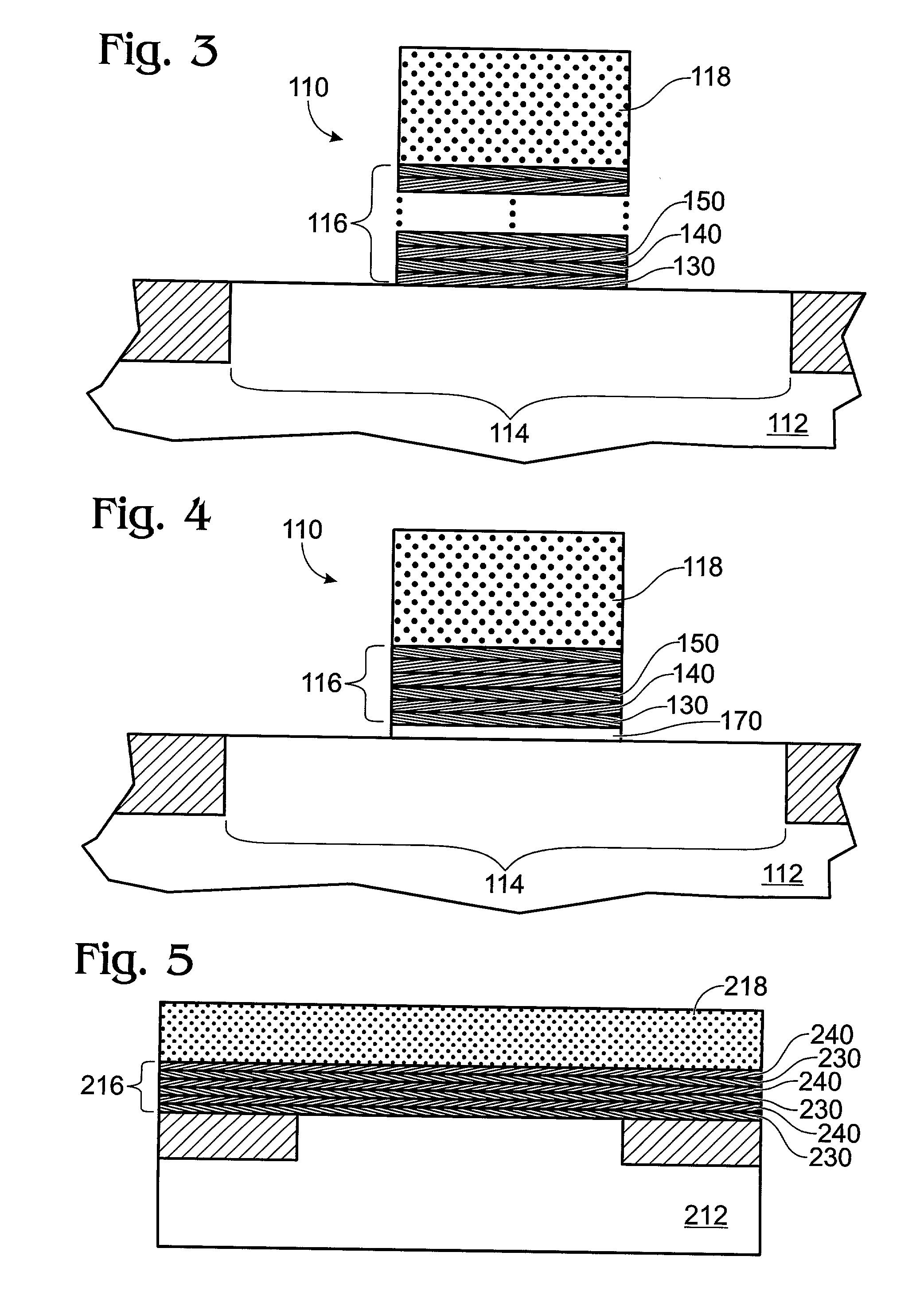
[0029] Referring now to the drawings, which are for illustration purposes (not to scale), FIG. 1 shows a common prior art integrated circuit (IC) structure, specifically a MOS transistor gate structure 10. MOS transistor gate structure 10 formed on a semiconductor substrate 12 above an active area 14 containing a channel region 15. MOS transistor gate structure 10 has a silicon dioxide dielectric layer 16 located above channel region 15 having a width. An electrode 18, which is typically doped polysilicon, is formed above the dielectric layer 16 to complete the gate structure 10.

[0030] A completed MOS transistor will also include source region 21, drain region 23 and field isolation region 27, which are illustrated in FIG. 1 and in some other figures. But, these features will not be further described or identified as they are well known to those skilled in the art. Throughout the remainder of this description structures analogous to the MOS transistor gate structure 10 will often be...


PUM


Abstract

A multilayer dielectric stack is provided which has alternating layers of a high-k material and an interposing material. The presence of the interposing material and the thinness of the high-k material layers reduces or eliminate effects of crystallization within the high-k material, even at relatively high annealing temperatures. The high-k dielectric layers are a metal oxide of preferably zirconium or hafnium. The interposing layers are preferably amorphous aluminum oxide, aluminum nitride, or silicon nitride. Because the layers reduce the effects of crystalline structures within individual layers, the overall tunneling current is reduced. Also provided are atomic layer deposition, sputtering, and evaporation as methods of depositing desired materials for forming the above-mentioned multilayer dielectric stack.

Description

BACKGROUND OF THE INVENTION[0001] The present invention relates generally to integrated circuit (IC) fabrication processes and, more particularly, to a multilayer dielectric stack, and a method for producing such a stack.[0002] Current Si VLSI technology uses SiO.sub.2 as the gate dielectric in MOS devices. As device dimensions continue to scale down, the thickness of the SiO.sub.2 layer must also decrease to maintain the same capacitance between the gate and channel regions. Thicknesses of less than 2 nanometers (nm) are expected in the future. However, the occurrence of high tunneling current through such thin layers of SiO.sub.2 requires that alternate materials be considered. Materials with high dielectric constants would permit gate dielectric layers to be made thicker, and so alleviate the tunneling current problem. These so-called high-k dielectric films are defined herein as having a high dielectric constant relative to silicon dioxide. Typically, silicon dioxide has a diele...

Claims


Application Information

Patent Timeline
IPC IPC(8): B82B1/00H01L29/78H01L21/28H01L21/335H01L21/336H01L21/8246H01L27/105H01L29/51
CPCH01L21/28185H01L21/28194H01L21/28202H01L29/513H01L29/517H01L29/518H01L29/66583H01L21/18
Inventor MA, YANJUNONO, YOSHI
Owner SHARP LAB OF AMERICA INC
Why Eureka
Try Eureka